Intel386™ EX EMBEDDED MICROPROCESSOR USER’S MANUAL
6-2
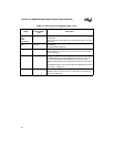
• Data status pins indicate that data is available on the data bus for a write (WR#) or that the
processor is ready to accept data for a read (RD#). These pins are available so that certain
system configurations can easily connect the processor directly to memory or I/O without
external logic.
• Bus control pins allow external logic to control the bus cycle on a cycle-by-cycle basis:
— READY# indicates that internal logic has completed the current bus cycle or that
external hardware has terminated it.
— NA# requests the next address to be put on the bus during a pipelined bus cycle.
— BS8# indicates that the current bus transaction is for an 8-bit data bus.
The remaining external bus pins interface to external bus masters and external logic for transfer-
ring control of the bus.
• An external bus master activates the HOLD pin to request the external bus.
— The internal bus arbiter arbitrates between the HOLD input and other potential requests
(DMA Units 0 and 1, Refresh Control Unit) based on their priorities.
— When another unit has control of the bus, the bus is released to the external bus master
based on the arbiter’s arbitration scheme (refer to “Bus Control Arbitration” on page
12-9 for information on internal bus masters also controlled by the internal bus arbiter
and the arbitration protocol used by the arbiter).
— When the core has control of the bus, the arbiter passes the request on to the core by
asserting the core HOLD signal.
— The core finishes the current nonlocked bus transfer and releases the bus signals.
— The core asserts the core HLDA signal to indicate that the bus has been released.
— The arbiter then asserts the HLDA pin to indicate to the external bus master that the bus
has been released.


