Intel386™ EX EMBEDDED MICROPROCESSOR USER’S MANUAL
6-4
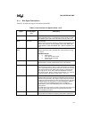
M/IO#
D/C#
W/R#
REFRESH#
Device pins Bus Cycle Definition Signals (Memory/IO, Data/Control, Write/Read,
and Refresh):
These four status outputs define the current bus cycle type, as shown
in Table 6-2.
NA# Device pin Next Address:
Requests address pipelining.
RD# Device pin Read Enable:
Indicates that the current bus cycle is a read cycle and the data bus is
able to accept data.
READY# Device pin Ready:
This bidirectional pin is used to terminate the current bus cycle. The
processor drives READY# when LBA# is active. The processor
samples the READY# pin at the falling edge of Phase 2 of T2, T2P or
T2i.
The READY# signal is also used to deassert the WR# signal (Refer to
“Write Cycle” on page 6-16).
WR# Device pin Write Enable:
Indicates that the current bus cycle is a write cycle and valid data is
present on the data bus.
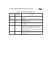
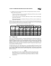
Table 6-1. Bus Interface Unit Signals (Sheet 2 of 2)
Signal
Device Pin or
Internal Signal
only
Description


