18-3
JTAG TEST-LOGIC UNIT
18.2 TEST-LOGIC UNIT OPERATION
18.2.1 Test Access Port (TAP)
The test access port consists of five dedicated pins (four inputs and one output). It is through these
pins that all communication with the test-logic unit takes place. This unit has its own clock (TCK)
and reset (TRST#) pins, so it is independent of the rest of the device. The test-logic unit can read
or write its registers even if the rest of the device is in reset or powerdown.
CAUTION
The JTAG Test-Logic Unit must be reset upon power-up using the TRST# pin.
(To do this, invert the RESET signal and send this inverted RESET to the
TRST# pin). If this is not done, the processor may power-up with the JTAG
test-logic unit in control of the device pins, and the system does not initialize
properly.
The test-logic unit allows you to shift test instructions and test data into the device and to read the
results of the test. A tester (that is, an external bus master such as automatic test equipment or a
component that interfaces to a higher-level test bus) controls the TAP controller’s operation by
applying signals to the clock (TCK) and test-mode-select (TMS) inputs. Instructions and data are
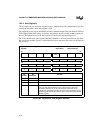
shifted serially from the test-data input (TDI) to the test-data output (TDO). Table 18-1 describes
the test access port pins.
Table 18-1. Test Access Port Dedicated Pins
Pin
Name
Description
TCK Test Clock Input:
Provides the clock input for the test-logic unit. An external signal must provide a maximum
input frequency of one-half the CLK2 input frequency. TCK is driven by the test-logic unit’s
control circuitry.
TDI Test Data Input:
Serial input for test instructions and data. Sampled on the rising edge of TCK; valid only when
either the instruction register or a data register is being serially loaded (SHIFT-IR, SHIFT-DR).
TDO Test Data Output:
Serial output for test instructions and data. TDO shifts out the contents of the instruction
register or the selected data register (LSB first) on the falling edge of TCK. If serial shifting is
not taking place, TDO floats.
TMS Test Mode Select Input:
Controls the sequence of the TAP controller’s states. Sampled on the rising edge of TCK.
TRST# Test Reset Input:
Resets the TAP controller. Asynchronously clears the data registers and initializes the
instruction register to 0010 (the IDCODE instruction opcode).
NOTE: The JTAG Test-Logic Unit must be reset upon power-up using the TRST# pin. If this is not done
the processor may power-up with the JTAG test-logic unit in control of the device pins, and the
system does not initialize properly.


