


Intel386™ EX EMBEDDED MICROPROCESSOR USER’S MANUAL
6-10
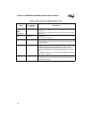
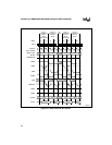
• A doubleword (32-bit) transfer at (byte) address 03H requires three transfers, one word
transfer and two byte transfers:
— The first word transfer activates word address 04H and uses D15:0 (to write or read the
middle 2 bytes of the 32-bit doubleword)
— The next transfer activates word address 06H and uses D7:0 (to write or read the upper
byte of the 32-bit word)
— The last transfer activates word address 02H and uses D15:8 (to write or read the lower
byte of the 32-bit word)
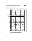
Table 6-3 shows the sequence of bus cycles for all possible alignments and operand length trans-
fers. Even though nonaligned transfers are transparent to a program, they are slower than aligned
transfers (due to the extra cycles needed) and should be avoided.
6.2.4 Ready Logic
A bus cycle is terminated externally by asserting the READY# pin or internally by either an in-
ternal peripheral or the Chip-select Unit’s wait-state logic. When an access is to an internal pe-
ripheral, the address also goes out to the external bus. When an external device incorrectly
decodes a match to the address and drives the READY# pin, contention occurs on the signal. The
LBA# pin should be used to alleviate the possibility of contention on the READY# pin. The
READY# pin is an output of the processor whenever LBA# is asserted and an input to the pro-
cessor whenever LBA# is deasserted.
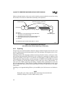
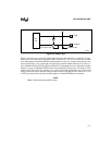
The LBA# pin becomes active when the processor is generating the READY# internally. Figure
6-3 shows the implementation of the READY# signal using the LBA# signal. If you wish to sim-
plify decoding of address space and overlap internal I/O registers, you need to provide external
logic to monitor LBA# and end the bus cycle externally when the processor generates the
READY# internally.
NOTE
Since LBA# may be used as an output-enable by both the internal and external
READY# buffers, care must be taken in selecting the external READY# buffer
to minimize contention on the READY# signal caused by differences in buffer
characteristics.
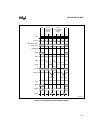
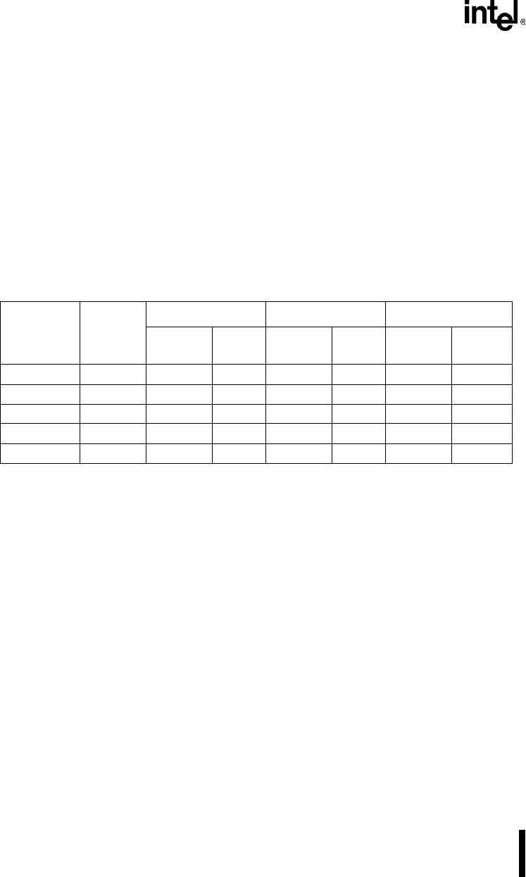
Table 6-3. Sequence of Nonaligned Bus Transfers
Transfer
Type
Physical
Address
First Cycle Second Cycle Third Cycle
Address
Bus
Byte
Enable
Address
Bus
Byte
Enable
Address
Bus
Byte
Enable
word 4N+1 4N BHE# 4N+2 BLE#
word 4N+3 4N+4 BLE# 4N+2 BHE#
doubleword 4N+1 4N+4 BLE# 4N BHE# 4N+2 both
doubleword 4N+2 4N+4 both 4N+2 both
doubleword 4N+3 4N+4 both 4N+6 BLE# 4N+3 BHE#