15-5
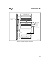
REFRESH CONTROL UNIT
The 13-bit address counter is a combination of a binary counter and a 7-bit linear-feedback shift
register. The binary counter produces address bits A13:8 and the linear-feedback shift register
produces address bits A7:1. The shift register nonsequentially produces all 128 (2
7
) possible com-
binations. Each time the lower seven bits cycle through all 128 combinations, the binary counter
increments the upper 6 bits. This continues until the 13-bit address counter cycles through 8192
(2
13
) address combinations. The counter then rolls over to its original value and the process re-
peats.
15.2.4 Bus Arbitration
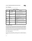
Because the two DMA channels, an external device (via the HOLD pin), and the refresh control
unit can all request bus control, bus control priority must be arbitrated. Refresh requests always
have the highest priority. “Bus Control Arbitration” on page 12-9 discusses the priority structure
of the other bus control requests.)
When a refresh occurs while a DMA channel is performing a transfer, the RCU “steals” a bus cy-
cle to perform a refresh. An external device can gain bus control through either the HOLD signal
or the DMA cascade mode. In this case, a refresh request causes the HLDA or DMACKn# signal
to be deasserted. When this happens, the external device should deassert its request line (HOLD
or DRQn) to allow the RCU to perform a refresh cycle. The refresh cycle is not executed until the
external device deasserts its request. If the external device reasserts its request signal before the
RCU completes the refresh cycle, bus control is given back to the external device after the refresh
cycle completes, without further arbitration.
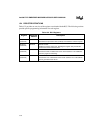
15.3 RCU OPERATION
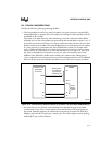
The following steps describe the basic refresh cycle, which is initiated every time the interval
counter reaches one.
1. The interval timer unit asserts the timeout signal and reloads the interval counter with the
refresh clock interval register value. The interval counter decrements on each succeeding
processor clock falling edge.
2. The RCU requests bus ownership.
3. Bus ownership is given to the control unit.
4. The control unit asserts the REFRESH# signal and a bus memory read cycle (with neither
Byte-enable signal active) is executed with the address supplied by the RCU.
5. The DRAM controller asserts RAS#, latching the row address inside the DRAM device.
This refreshes the row.
6. The control unit deasserts REFRESH#, and the process repeats from step 1 when the
interval counter reaches one again.
Once enabled, the DRAM refresh process continues until you reprogram the RCU, a reset occurs,
or the processor enters powerdown mode.


