6-23
BUS INTERFACE UNIT
A complete discussion of the considerations for using pipelining can be found in the Intel386
™
SX Processor datasheet (order number 240187) or the Intel386™ SX Microprocessor Hardware
Reference Manual (order number 240332).
6.3.4 Interrupt Acknowledge Cycle
An interrupt causes the processor to suspend execution of the current program and execute in-
structions from another program called an interrupt service routine. Interrupts are described in
Chapter 9.
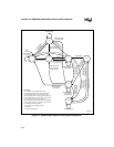
The interrupt control unit coordinates the interrupts of several devices, internal and external. It
contains two 82C59A programmable interrupt controllers (PICs) connected in cascade. The slave
82C59A module controls up to five internal interrupt sources and up to four external interrupt
sources depending upon the configuration programmed. The master 82C59A module controls the
slave 82C59A, three internal interrupt sources and up to six external interrupt sources depending
upon the configuration programmed. When a device signals an interrupt request, the interrupt
control unit activates the processor’s INTR input.
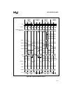
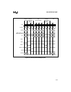
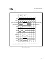
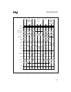
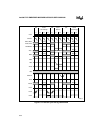
Interrupt acknowledge cycles are special bus cycles that enable the interrupt control unit to output
a service-routine vector onto the data bus. The processor performs two back-to-back interrupt ac-
knowledge cycles in response to an active INTR input (as long as the interrupt flag is enabled).
Interrupt acknowledge cycles are similar to regular bus cycles in that the processor initiates each
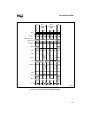
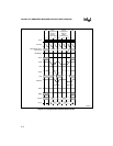
bus cycle and an active READY# terminates each bus cycle. The cycles are shown in Figure 6-9.
The sequence of signals for an interrupt acknowledge cycle is as follows:
1. The address and status signals are driven active and ADS# is driven low to start each bus
cycle.
• Status signals M/IO#, D/C#, and W/R# are low to indicate an interrupt acknowledge
bus cycle. These signals must be decoded to generate the INTA input signal for an
external 82C59A, if an external cascaded 82C59A is used. The REFRESH# signal is
high.
• LOCK# is active from the beginning of the first cycle to the end of the second. HOLD
requests from other bus masters are not recognized until after the second interrupt
acknowledge cycle is completed.
• NA# is ignored.
• The byte address driven during the first cycle is 4; during the second cycle the byte
address is 0. BHE# is high, BLE# is low, and A25:3 and A1 are low for both cycles;
A2 is high for the first cycle and low for the second. If the CAS enable bit in the
interrupt control unit’s configuration register is set (INTCFG.7=1), address bits
A18:16 reflect the status of the CAS lines. The CAS lines go valid at the rising edge
of PH2 of the T1 state of the first interrupt acknowledge cycle. They then go invalid
at the rising edge of PH2 of the next Ti state. At the rising edge of PH2 of the T1 state
of the second interrupt acknowledge cycle, the CAS lines go valid again. They then
go invalid at the rising edge of PH2 of the next Ti state.


