6-7
BUS INTERFACE UNIT
6.2.1 Bus States
The processor uses a double-frequency clock input (CLK2). This clock is internally divided by
two and synchronized to the falling edge of RESET (see Figure 8-2 in Chapter 8) to generate the
internal processor clock signal. Each processor clock cycle is two CLK2 cycles wide.
Each bus cycle is composed of at least two bus states: T1 and T2. Each bus state in turn consists
of two CLK2 cycles, which can be thought of as Phase 1 (PH1) and Phase 2 (PH2) of the bus state.
External circuitry can use the CLKOUT signal (generated by the processor) to synchronize itself
with the processor. This signal is a replica of the PH1P clock, which is the PH1 clock that is used
by the internal peripherals. (For more information, refer to Chapter 8, “CLOCK AND POWER
MANAGEMENT UNIT.”) The CLKOUT signal is used as a phase status indicator for external
circuitry. All device inputs are sampled and outputs are activated at CLK2 rising edges. This
makes synchronous circuit design easy through the use of rising-edge-triggered, registered logic
(such as PALs, PLDs and EPLDs).
Many signals are sampled by the processor on every other CLK2 rising edge: some are sampled
on the CLK2 edge when CLKOUT is going high, while others are sampled on the CLK2 edge
when PH1 is going low.
The maximum data transfer rate for a bus operation is 16 bits for every two processor clock cycles
(two CLKOUT cycles).
During the first bus state (T1), address and bus status pins go active. During the second bus state
(T2), external logic and devices respond.
• When the READY# input is sampled low at the falling edge of PH2 in T2, the bus cycle
terminates.
• When READY# is high when sampled, the bus cycle continues for an additional T2 state,
called a wait-state, and READY# is sampled again. This process continues until READY#
is sampled active, at which point the bus cycle terminates.
Wait-states are added until READY# is sampled low. READY# is sampled externally when the
LBA# signal is inactive. When the LBA# signal is active, the processor is generating the
READY# signal internally. READY# can be generated internally by either an internal peripheral
or the chip-select unit’s wait-state generator. When no bus cycles are needed (no bus requests are
pending), the processor remains in the idle bus state, Ti. The relationship between T1, T2, and Ti
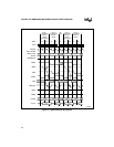
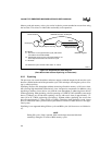
is shown in Figure 6-2.
From an idle bus, the processor begins a bus cycle by first driving a valid address and bus cycle
status onto the address and status buses. Hardware can distinguish the difference between an idle
cycle and an active bus cycle by the address strobe (ADS#) signal being driven active. The ADS#
signal remains active for only the first T-state of the bus cycle, while the address signals and status
signals remain active until the bus cycle is terminated by an active READY# signal or the bus
cycle is pipelined. Pipelined bus cycles are discussed in “Pipelining” on page 6-8. Basic bus cy-
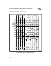
cles are illustrated in Figure 6-1. The bus status signals indicate the type of bus cycle the proces-
sor is executing. Notice that the signal combinations marked as invalid states may occur when the
bus is idle and ADS# is inactive.


