5-11
DEVICE CONFIGURATION
5.2.3 Timer/counter Unit Configuration
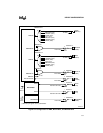
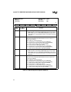
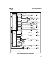
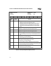
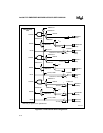
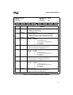
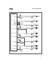
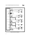
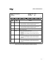
The three-channel Timer/counter Unit (TCU) and its configuration register (TMRCFG) are
shown in Figure 5-6 and Figure 5-7. The clock inputs can be external signals (TMRCLK2:0) or
the on-chip programmable clock (PSCLK). All clock inputs can be held low by programming bits
in the TMRCFG register. The gate inputs can be controlled through software using TMRCFG.6
and the appropriate GTnCON bits in the TMRCFG register. Several of the timer signals go to the
interrupt control unit (see Figure 5-4).
The Timer/counter0 and Timer/counter1 signals are selected individually. In contrast, the Tim-
er/counter2 signals (TMRCLK2, TMRGATE2, TMROUT2) are selected as a group. Note that us-
ing the Timer/counter2 signals precludes use of the coprocessor signals (PEREQ, BUSY#, and
ERROR#).
The CLKINn and GATEn inputs of Timer/counter0 and Timer/counter1 are routed directly to
shared input pins, TMRCLK0/INT4, TMRCLK1/INT6, TMRGATE0/INT5 and
TMRGATE1/INT7. The OUTn inputs of these two counters can be connected to pins
TMROUT0/INT9/P3.0 and TMROUT1/INT8/P3.1 respectively, using bits in registers P3CFG
and INTCFG.


