


14-15
CHIP-SELECT UNIT
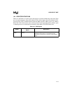
14.4.1 Pin Configuration Register (PINCFG)
Use PINCFG bits 6 and 4 to connect the CS6# and CS5# signals to package pins.
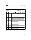
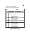
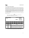
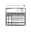
Figure 14-4. Pin Configuration Register (PINCFG)
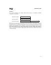
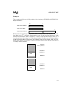
Pin Configuration
PINCFG
(read/write)
Expanded Addr:
ISA Addr:
Reset State:
F826H
—
00H
7 0
— PM6 PM5 PM4 PM3 PM2 PM1 PM0
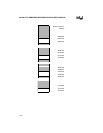
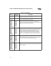
Bit
Number
Bit
Mnemonic
Function
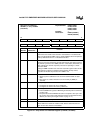
7 — Reserved. This bit is undefined; for compatibility with future devices, do
not modify this bit.
6 PM6 Pin Mode:
0 = Selects CS6# at the package pin.
1 = Selects REFRESH# at the package pin.
5 PM5 Pin Mode:
0 = Selects the coprocessor signals, PEREQ, BUSY#, and ERROR#, at
the package pins.
1 = Selects the timer control unit signals, TMROUT2, TMRCLK2, and
TMRGATE2, at the package pins.
4 PM4 Pin Mode:
0 = Selects DACK0# at the package pin.
1 = Selects CS5# at the package pin.
3 PM3 Pin Mode:
0 = Selects EOP# at the package pin.
1 = Selects CTS1# at the package pin.
2 PM2 Pin Mode:
0 = Selects DACK1# at the package pin.
1 = Selects TXD1 at the package pin.
1 PM1 Pin Mode:
0 = Selects SRXCLK at the package pin.
1 = Selects DTR1# at the package pin.
0 PM0 Pin Mode:
0 = Selects SSIOTX at the package pin.
1 = Selects RTS1# at the package pin.