Intel386™ EX EMBEDDED MICROPROCESSOR USER’S MANUAL
9-18
9.3.1 Port 3 Configuration Register (P3CFG)
Use the P3CFG register to connect the interrupt request signals (INT3:0) to the package pins.
These signals are multiplexed with port 3 signals, P3.5–2. Connecting a port 3 signal to the pack-
age pin also connects V
SS
to the corresponding master’s IR signal, disabling the signal.
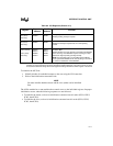
Figure 9-6. Port 3 Configuration Register (P3CFG)
Port 3 Configuration
P3CFG
(read/write)
Expanded Addr:
ISA Addr:
Reset State:
F824H
—
00H
7 0
PM7 PM6 PM5 PM4 PM3 PM2 PM1 PM0
Bit
Number
Bit
Mnemonic
Function
7 PM7 Pin Mode:
0 = Selects P3.7 at the package pin.
1 = Selects COMCLK at the package pin.
6 PM6 Pin Mode:
0 = Selects P3.6 at the package pin.
1 = Selects PWRDOWN at the package pin.
5 PM5 Pin Mode:
0 = Selects P3.5 at the package pin.
1 = Connects master IR7 to the package pin (INT3).
4 PM4 Pin Mode:
0 = Selects P3.4 at the package pin.
1 = Connects master IR6 to the package pin (INT2).
3 PM3 Pin Mode:
0 = Selects P3.3 at the package pin.
1 = Connects master IR5 to the package pin (INT1).
2 PM2 Pin Mode:
0 = Selects P3.2 at the package pin.
1 = Connects master IR1 to the package pin (INT0).
1 PM1 Pin Mode:
See Table 5-1 on page 5-8 for all the PM1 configuration options.
0 PM0 Pin Mode:
See Table 5-1 on page 5-8 for all the PM0 configuration options.


