Memory Management 7-19
7.8.1 Storage Attribute Control Registers
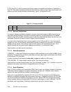
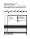
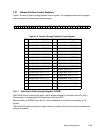
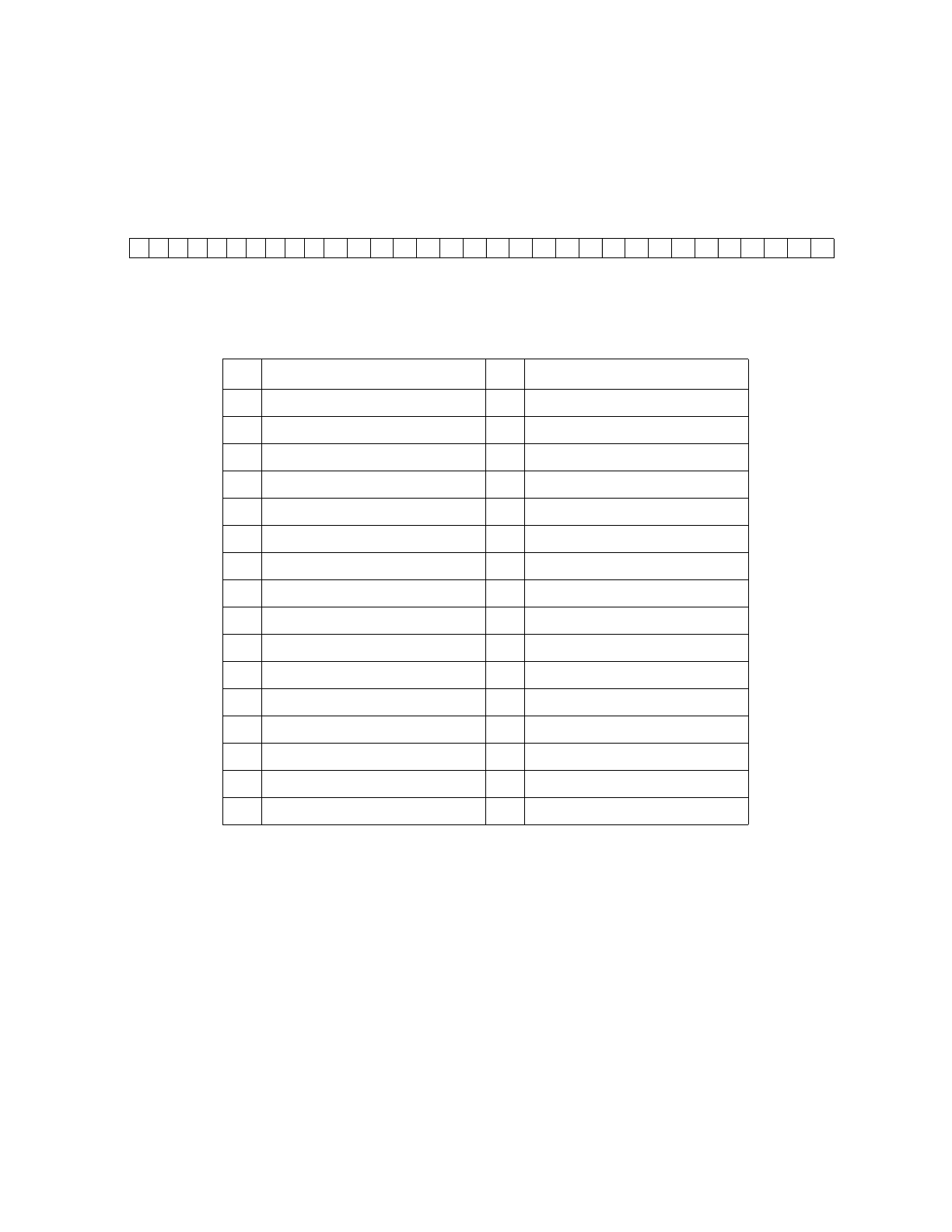
Figure 7-6 shows a generic storage attribute control register. The storage attribute control registers
have the same bit numbering and address ranges.
7.8.1.1 Data Cache Write-through Register (DCWR)
The DCWR controls write-through policy (the W storage attribute) for the data cache unit (DCU).
Write-through is not applicable to the instruction cache unit (ICU).
After any reset, all DCWR bits are set to 0, which establishes a write-back write strategy for all
regions.
The PowerPC Architecture does not support memory models in which write-through is enabled and
caching is inhibited.
Figure 7-6. Generic Storage Attribute Control Register
Bit Address Range Bit Address Range
0 0x0000 0000–0x07FF FFFF 16 0x8000 0000 –0x87FF FFFF
1 0x0800 0000–0x0FFF FFFF 17 0x8800 0000 –0x8FFF FFFF
2 0x1000 0000–0x17FF FFFF 18 0x9000 0000 –0x97FF FFFF
3 0x1800 0000–0x1FFF FFFF 19 0x9800 0000 –0x9FFF FFFF
4 0x2000 0000–0x27FF FFFF 20 0xA000 0000 –0xA7FF FFFF
5 0x2800 0000–0x2FFF FFFF 21 0xA800 0000 –0xAFFF FFFF
6 0x3000 0000–0x37FF FFFF 22 0xB000 0000 –0xB7FF FFFF
7 0x3800 0000–0x3FFF FFFF 23 0xB800 0000 –0xBFFF FFFF
8 0x4000 0000–0x47FF FFFF 24 0xC000 0000 –0xC7FF FFFF
9 0x4800 0000–0x4FFF FFFF 25 0xC800 0000 –0xCFFF FFFF
10 0x5000 0000–0x57FF FFFF 26 0xD000 0000 –0xD7FF FFFF
11 0x5800 0000–0x5FFF FFFF 27 0xD800 0000 –0xDFFF FFFF
12 0x6000 0000–0x67FF FFFF 28 0xE000 0000 –0xE7FF FFFF
13 0x6800 0000–0x6FFF FFFF 29 0xE800 0000 –0xEFFF FFFF
14 0x7000 0000–0x77FF FFFF 30 0xF000 0000 –0xF7FF FFFF
15 0x7800 0000–0x7FFF FFFF 31 0xF800 0000 –0xFFFF FFFF
0 1 2 3 4 5 6 7 8 9 10 11 12 13 14 15 16 17 18 19 20 21 22 23 24 25 26 27 28 29 30 31


