


8-20 PPC405 Core User’s Manual
specifications for vendor-specific extensions, are compatible with standard JTAG hardware for
boundary-scan system testing.
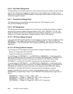
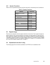
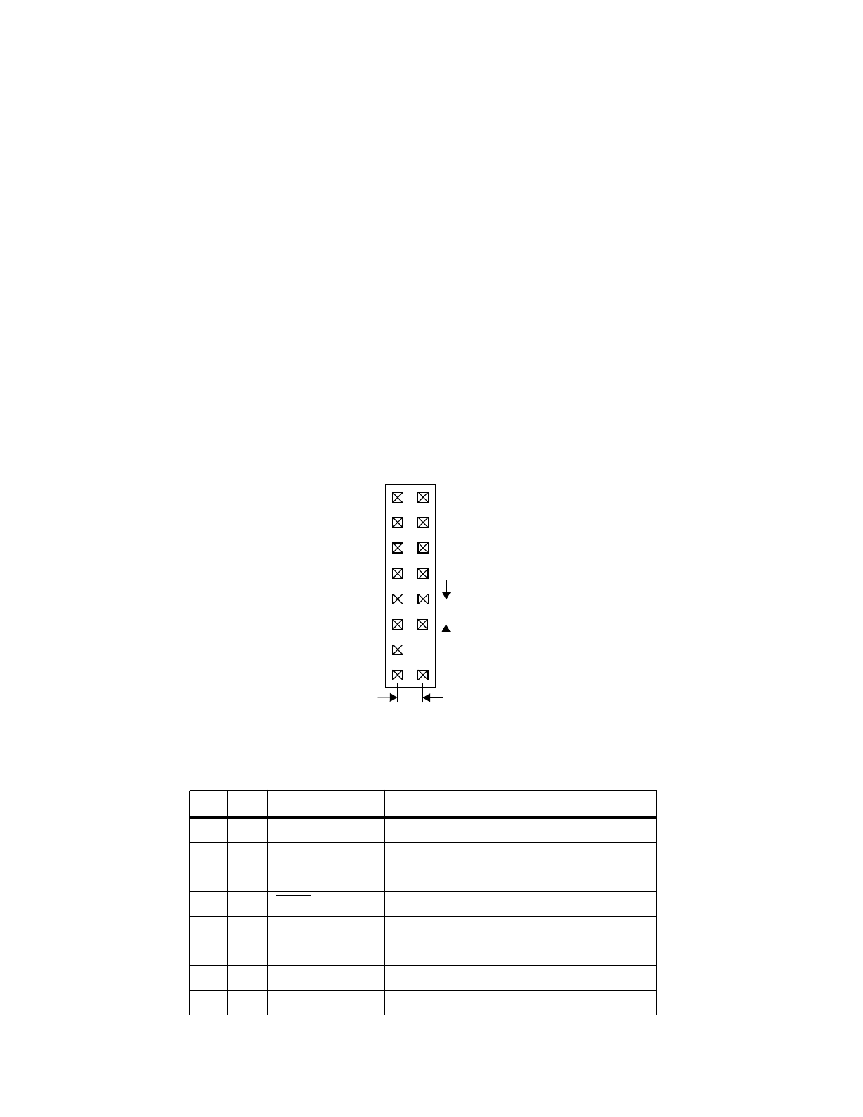
8.7 JTAG Connector
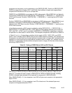
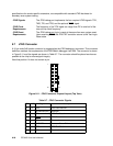
A 16-pin male 2x8 header connector is suggested as the JTAG debug port connector. This connector
definition matches the requirements of the RISCWatch debugger from IBM. The connector is shown
in Figure 8-11 and the signals are shown in Table 8-7. The connector should be placed as close as
possible to the chip to ensure signal integrity.
Note that position 14 does not contain a pin.
JTAG Signals The JTAG debug port implements the four required JTAG signals: TCK,
TMS, TDI, and TDO, and the optional
TRST signal.
JTAG Clock
Requirements
The frequency of the TCK signal can range from DC to one-half of the
internal chip clock frequency.
JTAG Reset
Requirements
The JTAG debug port logic is reset at the same time as a system reset.
Upon receiving TRST, the JTAG TAP controller returns to the Test-Logic
Reset state.
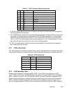
Table 8-7. JTAG Connector Signals
Pin I/O Signal Description
1 O TDO JTAG Test Data Out
2 No connect (NC) Reserved
3 I TDI
1
JTAG Test Data In
4
TRST JTAG Reset
5 NC Reserved
6 +POWER
2
Processor Power OK
7 I TCK
3
JTAG Test Clock
8 NC Reserved
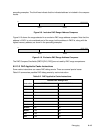
1
0.1"
0.1"
2
KEY
15
16
Figure 8-11. JTAG Connector Physical Layout (Top View)