


1-4 PPC405 Core User’s Manual
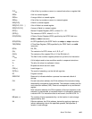
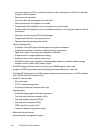
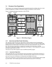
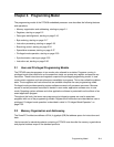
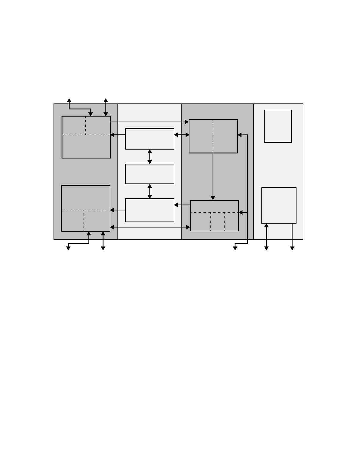
1.4 Processor Core Organization
The processor core consists of a 5-stage pipeline, separate instruction and data cache units, virtual
memory management unit (MMU), three timers, debug, and interfaces to other functions.
Figure 1-1 illustrates the logical organization of the PPC405.
1.4.1 Instruction and Data Cache Controllers
The instruction cache unit (ICU) and data cache unit (DCU) enable concurrent accesses and
minimize pipeline stalls. The storage capacity of the cache units, which can range from 0KB–32KB,
depends upon the implementation. Both cache units are two-way set-associative, use a 32-byte line
size. The instruction set provides a rich assortment of cache control instructions, including
instructions to read tag information and data arrays. See Chapter 4, “Cache Operations,” for detailed
information about the ICU and DCU.
The cache units are PLB-compliant for use in the IBM Core+ASIC program.
1.4.1.1 Instruction Cache Unit
The ICU provides one or two instructions per cycle to the execution unit (EXU) over a 64-bit bus. A
line buffer (built into the output of the array for manufacturing test) enables the ICU to be accessed
only once for every four instructions, to reduce power consumption by the array.
The ICU can forward any or all of the words of a line fill to the EXU to minimize pipeline stalls caused
by cache misses. The ICU aborts speculative fetches abandoned by the EXU, eliminating
405 CPU
3-Element
Fetch
Queue
(PFB1,
PFB0,
DCD)
Fetch
and
Decode
Logic
Instruction Shadow
TLB
(4 Entry)
Unified TLB
(64 Entry)
Execute Unit (EXU)
32 x 32
ALU
MAC
GPR
Data Shadow
TLB
(8 Entry)
Timers
(FIT,
PIT,
Watchdog)
Timers
MMU
Cache Units
&
Debug
APU/FPU
Debug Logic
(4 IAC,
2 DAC,
2 DVC)
JTAG Instruction
Trace
Data
D-Cache D-Cache
PLB Master Data
Interface OCM
Cache
Unit
ControllerArray
PLB Master Instruction
I-Cache I-Cache
Instruction
Interface OCM
ControllerArray
Cache
Unit
Figure 1-1. PPC405 Block Diagram