


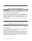
8-10 PPC405 Core User’s Manual
8.5.5 Data Value Compare Registers (DVC1–DVC2)
The PPC405 can take a debug event upon storage or cache references to addresses specified in the
DAC registers, that also require the data at that address to match the value specified in the DVC
registers. The data address compare for a DVC events works the same as for a DAC event. Cache
operations do not cause DVC events. If the data at the address specified matches the value in the
corresponding DVC register a DVC event will occur. The fields DBCR1[DV1M, DV2M] control how the
data value are compared.
Errors related to execution of storage reference or cache instructions prevent DVC debug events.
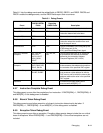
8.5.6 Debug Events
Debug events, enabled and configured by DBCR0 and DBCR1 and recorded in the DBSR, cause
debug operations. A debug event occurs when an event listed in Table 8-1 on page 8-11 is detected.
The debug operation is performed after the debug event.
In internal debug mode, the processor generates a debug interrupt when a debug event occurs. In
external debug mode, the processor stops when a debug event occurs. When internal and external
debug mode are both enabled, the processor stops on a debug event with the debug interrupt
pending. When external and internal debug mode are both disabled, and debug wait mode is enabled
the processor stops, but can be restarted by an interrupt. When all debug modes are disabled, debug
events are recorded in the DBSR, but no action is taken.
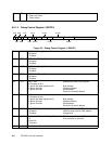
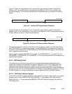
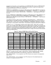
Figure 8-5. Data Address Compare Registers (DAC1–DAC2)
0:31 Data Address Compare (DAC) byte
address
DBCR0[D1S] determines which address
bits are examined.
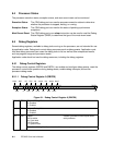
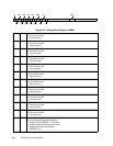
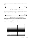
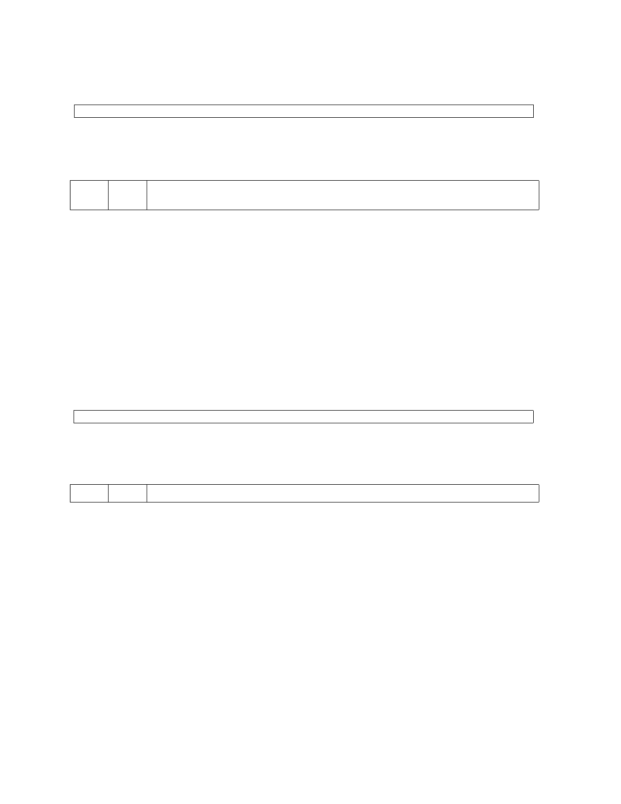
Figure 8-6. Data Value Compare Registers (DVC1–DVC2)
0:31 Data Value to Compare
0 31
0 31