8-16 PPC405 Core User’s Manual
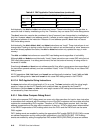
Architecturally, the dcbi and dcbz instructions are “stores.” These instructions can change data, or
cause the loss of data by invalidating a dirty line. Therefore, they can cause DAC-write debug events.
The dccci instruction can also be considered a “store” because it can change data by invalidating a
dirty line. However, dccci is not address-specific; it affects an entire congruence class regardless of
the operand address of the instruction. Because it is not address-specific, dccci does not cause
DAC-write debug events.
Architecturally, the dcbt, dcbtst, dcbf, and dcbst instructions are “loads.” These instructions do not
change data. Flushing or storing a cache line from the cache is not architecturally a “store” because a
store had already updated the cache; the dcbf or dcbst instruction only updates the copy in main
memory.
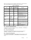
The dcbt and dcbtst instructions can cause DAC-read debug events regardless of cachability.
Although dcbf and dcbst are architecturally “loads,” these instructions can create DAC-write (but not
DAC-read) debug events. In a debug environment, the fact that external memory is being written is
the event of interest.
Even though dcread and dccci are not address-specific (they affect a congruence class regardless of
the instruction operand address), and are considered “loads,” in the PPC405 they do not cause DAC
debug events.
All ICU operations (icbi, icbt, iccci, and icread) are architecturally treated as “loads.” icbi and icbt
cause DAC debug events. iccci and icread do not cause DAC debug events in the PPC405.
8.5.13.4 DAC Applied to String Instructions
An stswx instruction with a string length of 0 is a no-op. The lswx instruction with the string length
equal to 0 does not alter the RT operand with undefined data, as allowed by the PowerPC
Architecture. Neither stswx nor lswx with zero length causes a DAC debug event because storage is
not accessed by these instructions.
8.5.14 Data Value Compare Debug Event
A data value compare (DVC) debug event can occur only after execution of a load or store instruction
to an address that compares with the address in one of the DAC
n
registers and has a data value that
matches the corresponding DVC
n
register. Therefore, a DVC debug event requires both the data
address comparison and the data value comparison to be true. A DVCn debug event when enabled
in the DBCR1 supercedes a DACn debug event since the DVCn and the DACn both use the same
DACn register.
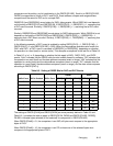
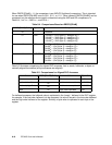
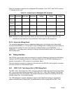
DVC1 debug events are enabled by setting the appropriate DAC enable DBCR1[D1R,D1W] to cause
an address comparison and by setting anybit combination in the DBCR1[DV1BE]. DVC2 debug
events are enabled by setting the appropriate DAC enable DBCR1[D2R,D2W] to cause an address
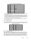
iccci No No
icread No No
Table 8-2. DAC Applied to Cache Instructions (continued)
Instruction
Possible DAC Debug Event
DAC-Read DAC-Write


