


1-8 PPC405 Core User’s Manual
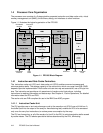
1.4.5.1 Processor Local Bus
The PLB-compliant interface provides separate 32-bit address and 64-bit data buses for the
instruction and data sides.
1.4.5.2 Device Control Register Bus
The Device Control Register (DCR) bus supports the attachment of on-chip registers for device
control.
These registers are accessed using the mfdcr and mtdcr instructions.
1.4.5.3 Clock and Power Management
This interface supports several methods of clock distribution and power management.
1.4.5.4 JTAG
The JTAG port is enhanced to support the attachment of a debug tool such as the RISCWatch
product from IBM Microelectronics. Through the JTAG test access port, a debug tool can single-step
the processor and interrogate internal processor state to facilitate software debugging. The
enhancements comply with the IEEE 1149.1 specification for vendor-specific extensions, and are
therefore compatible with standard JTAG hardware for boundary-scan system testing.
1.4.5.5 Interrupts
The processor core provides an interface to an on-chip interrupt controller that is logically outside the
core. The interrupt controller combines asynchronous interrupt inputs from on-chip and off-chip
sources and presents them to the core using a pair of interrupt signals: critical and non-critical. The
sources of asynchronous interrupts are external signals, the JTAG/debug unit, and any implemented
peripherals.
1.4.5.6 Auxiliary Processor Unit
The auxiliary processor unit (APU) interface supports the attachment of auxiliary processor hardware
and the implementation of the associated instructions for improved performance in specialized
applications.
1.4.5.7 On-Chip Memory
The on-chip memory (OCM) interface supports the implementation of instruction- and data-side
memory that can be accessed at performance levels matching the cache arrays.
1.4.6 Data Types
Processor core operands are bytes, halfwords, and words. Multiple words or strings of bytes can be
transferred using the load/store multiple and load/store string instructions. Data is represented in twos
complement notation or in unsigned fixed-point format.
The address of a multibyte operand is always the lowest memory address occupied by that operand.
Byte ordering can be selected as big endian (the lowest memory address of an operand contains its
most significant byte) or as little endian (the lowest memory address of an operand contains its least