Register Summary 10-1
Chapter 10. Register Summary
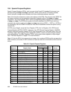
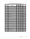
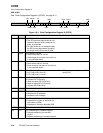
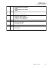
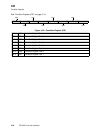
All registers contained in the PPC405 core are architected as 32-bits. Table 10-1 and Table 10-2
define the addressing required to access the registers. The pages following these tables define the bit
usage within each register.
The registers are grouped into categories, based on access mode: General Purpose Registers
(GPRs), Special Purpose Registers (SPRs), Time Base Registers (TBRs), the Machine State
Register (MSR), the Condition Register (CR), and, in standard products, Device Control Registers
(DCRs).
10.1 Reserved Registers
Any register numbers not listed in the tables which follow are
reserved,
and should be neither read
nor written. These reserved register numbers may be used for additional functions in future
processors.
10.2 Reserved Fields
For all registers having fields marked as reserved, the reserved fields should be written as
zero
and
read as
undefined
. That is, when writing to a reseved field, writea0tothefield. When reading from a
reserved field, ignore the field.
It is good coding practice to perform the initial write to a register with reserved fields as described in
the preceding paragraph, and to perform all subsequent writes to the register using a read-modify-
write strategy: read the register, alter desired fields with logical instructions, and then write the
register.
10.3 General Purpose Registers
The PPC405 core provides 32 General Purpose Registers (GPRs). The contents of these registers
can be loaded from memory using load instructions and stored to memory using store instructions.
GPRs are also addressed by all integer instructions.
10.4 Machine State Register and Condition Register
Because these registers are accessed using special instructions, they do not require addressing.
Table 10-1. PPC405 General Purpose Registers
Mnemonic Register Name
GPR Number
AccessDecimal Hex
R0–R31 General Purpose Register 0–31 0–31 0x0–0x1F Read/Write


