Vol. 3 11-11
MEMORY CACHE CONTROL
11.3.1 Buffering of Write Combining Memory Locations
Writes to the WC memory type are not cached in the typical sense of the word
cached. They are retained in an internal write combining buffer (WC buffer) that is
separate from the internal L1, L2, and L3 caches and the store buffer. The WC buffer
is not snooped and thus does not provide data coherency. Buffering of writes to WC
memory is done to allow software a small window of time to supply more modified
data to the WC buffer while remaining as non-intrusive to software as possible. The
buffering of writes to WC memory also causes data to be collapsed; that is, multiple
writes to the same memory location will leave the last data written in the location and
the other writes will be lost.
The size and structure of the WC buffer is not architecturally defined. For the Intel
Core 2 Duo, Intel Atom, Intel Core Duo, Pentium M, Pentium 4 and Intel Xeon proces-
sors; the WC buffer is made up of several 64-byte WC buffers. For the P6 family
processors, the WC buffer is made up of several 32-byte WC buffers.
When software begins writing to WC memory, the processor begins filling the WC
buffers one at a time. When one or more WC buffers has been filled, the processor
has the option of evicting the buffers to system memory. The protocol for evicting the
WC buffers is implementation dependent and should not be relied on by software for
system memory coherency. When using the WC memory type, software must be
sensitive to the fact that the writing of data to system memory is being delayed and
must deliberately empty the WC buffers when system memory coherency is
required.
Once the processor has started to evict data from the WC buffer into system
memory, it will make a bus-transaction style decision based on how much of the
buffer contains valid data. If the buffer is full (for example, all bytes are valid), the
processor will execute a burst-write transaction on the bus. This results in all 32
bytes (P6 family processors) or 64 bytes (Pentium 4 and more recent processor)
being transmitted on the data bus in a single burst transaction. If one or more of the
WC buffer’s bytes are invalid (for example, have not been written by software), the
processor will transmit the data to memory using “partial write” transactions (one
chunk at a time, where a “chunk” is 8 bytes).
This will result in a maximum of 4 partial write transactions (for P6 family processors)
or 8 partial write transactions (for the Pentium 4 and more recent processors) for one
WC buffer of data sent to memory.
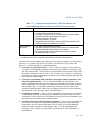
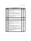
NOTE:
* Introduced in the Pentium III processor; not available in the Pentium Pro or Pentium II processors
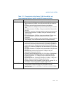
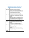
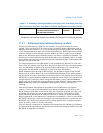
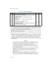
Table 11-3. Methods of Caching Available in Intel Core 2 Duo, Intel Atom, Intel Core
Duo, Pentium M, Pentium 4, Intel Xeon, P6 Family, and Pentium Processors (Contd.)
Memory Type Intel Core 2 Duo, Intel Atom, Intel
Core Duo, Pentium M, Pentium 4
and Intel Xeon Processors
P6 Family
Processors
Pentium
Processor


