


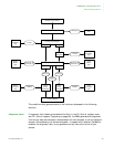

WORKING WITH THE CPU
Caches and write buffer
128 Hardware Reference NS9215
The caches use pseudo-random or round-robin replacement, selected by the RR
bit in R1: Control register.
Cache lockdown registers enable control over which cache ways are used for
allocation on a linefill, providing a mechanism for both lockdown and
controlling cache pollution.
The DCache stores the Physical Address Tag (PA tag) corresponding to each
DCache entry in the tag RAM for use during cache line write-backs, in addition
to the virtual address tag stored in the tag RAM. This means that the MMU is
not involved in DCache write-back operations, which removes the possibility of
TLB misses to the write-back address.
Cache maintenance operations provide efficient invalidation of:
–
The entire DCache or ICache
– Regions of the DCache or ICache
– Regions of virtual memory
Cache maintenance operations also provide for efficient cleaning and
invalidation of:
–
The entire DCache
– Regions of the DCache
– Regions of virtual memory
The latter allows DCache coherency to be efficiently maintained when small
code changes occur; for example, for self-modifying code and changes to
exception vectors.
Write buffer The write buffer is used for all writes to a noncachable bufferable region, write-
through region, and write misses to a write-back region. A separate buffer is
incorporated in the DCache for holding write-back data for cache line evictions or
cleaning of dirty cache lines.
The main write buffer has a 16-word data buffer and a four-address buffer.
The DCache write-back buffer has eight data word entries and a single address
entry.
The
MCR drain write buffer instruction enables both write buffers to be drained
under software control.
The
MCR wait -for-interrupt causes both write buffers to be drained, and the
ARM926EJ-S processor to be put into low-power state until an interrupt occurs.
Enabling the
caches
On reset, the ICache and DCache entries all are invalidated and the caches
disabled. The caches are not accessed for reads or writes. The caches are enabled
using the I, C, and M bits from the R1: Control register, and can be enabled
independently of one another.