


. . . . .
SERIAL CONTROL MODULE: SPI
SPI timing characteristics
www.digiembedded.com 443
Register
Register bit
assignment
. . . . . . . . . . . . . . . . . . . . . . . . . . . . . . . . . . . . . . . . . . . . . . . . . . . . . . . . . . . . . . . . . . . . . . . . . . . . . . . . . .
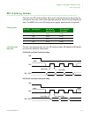
SPI timing characteristics
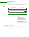
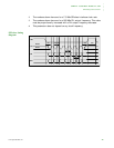
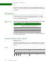
These are the guaranteed timing parameters for all four SPI clocking modes.
SPI master timing
parameters
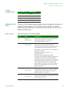
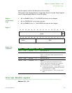
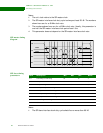
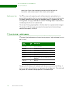
13 12 11 10 9 8 7 6 5 4 3 2 1 015 14
31 29 28 27 26 25 24 23 22 21 20 19 18 17 1630
Not used
Not used
TX_ IDLE RX_IDLE
Bits Access Mnemonic Reset Description
D31:02 R/W Not used 0 Write this field to 0.
D01 R/W1TC TX_IDLE 0 Transmit idle
Indicates that the transmitter has moved from the active
state to the idle state. The transmitter moves from the active
state to the idle state when the transmit FIFO is empty and
the transmitter is not actively shifting out data.
D00 R/W1TC RX_IDLE 0 Receive idle
Indicates that the receiver has moved from the active state
to the idle state. The receiver moves from the active state to
the idle state when a start bit has not been received within 4
bit periods of the previous stop bit.
Parm Description Min Max Unit Notes
S1 CS# falling to CLK rising 1 clock 1
S2 CLK period low time 12 13 ns 2
S3 CLK period high time 12 13 ns 2
S4 Data output setup to CLK rising 11 ns 3
S5 Data output hold from CLK rising 11 ns 3
S6 Data input setup to CLK rising 10 ns 4
S7 Data input hold from CLK rising 0 ns 4
S8 CLK falling to CS# rising 1 clock 1
S9 CS# deassertion time 4 clock 1