SERIAL CONTROL MODULE: SPI
Clock Generation register
440 Hardware Reference NS9215
. . . . . . . . . . . . . . . . . . . . . . . . . . . . . . . . . . . . . . . . . . . . . . . . . . . . . . . . . . . . . . . . . . . . . . . . . . . . . . . . . .
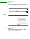
Clock Generation register
Address: 9003_1010
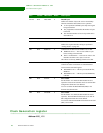
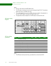
D11:08 R/W DISCARD 0 Discard bytes
Defines the number of bytes the receiver should drop
when the transmitter has initiated a new operation.
A new operation is defined by the chip select signal
being asserted low.
The programmed value defines the number of bytes
to discard.
The maximum number of receive bytes that can be
discarded is 14.
D07:06 R/W Not used 0 Write this field to 0.
D05:04 R/W MODE 0 SPI mode
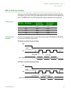
Defines the required interface timing as specified in
“Timing modes” on page 435.
D03 R/W RXBYTE 0 Controls how the SPI receiver handles receive data.
RXBYTE set to 0 — The receiver buffers 4 bytes
before writing to the RX FIFO.
Write a 1 to RXBYTE — The receiver writes to the
RX FIFO each time a new byte is received.
This allows low latency handling of SPI receive data.
D02 R/W BITORDR 0x0 Bit ordering
Controls the order in which bits are transmitted and
received in the serial shift register.
BITORDR set to 0 — Bits are processed LSB first,
MSB last.
BITORDR set to 1 — Bits are processed MSB first,
LSB last.
D01 R/W SLAVE 0 Slave enable
Set this field to 1 to enable the SPI module for slave
operation. The SLAVE field must not be set until all SPI
configuration fields have been defined.
You can set either the MASTER field (D00) or the
SLAVE field, but not both.
D00 R/W MASTER 0 Slave enable
Set this field to 1 to enable the SPI module for master
operation. The MASTER field must not be set until all
SPI configuration fields have been defined.
You can set either the MASTER field or the SLAVE field
(D01), but not both.
Bits Access Mnemonic Reset Description


