EXTERNAL DMA
DMA Peripheral Chip Select register
352 Hardware Reference NS9215
. . . . . . . . . . . . . . . . . . . . . . . . . . . . . . . . . . . . . . . . . . . . . . . . . . . . . . . . . . . . . . . . . . . . . . . . . . . . . . . . . .
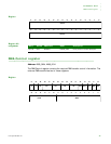
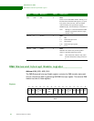
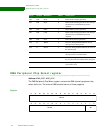
DMA Peripheral Chip Select register
Address: A080_000C, A080_001C
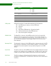
The DMA Peripheral Chip Select register contains the DMA channel peripheral chip
select definition. The external DMA module has two of these registers.
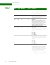
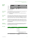
Register
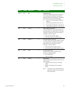
D24 R/W NCIE 0 Enable NCIP interrupt generation.
D23 R/W ECIE 0 Enable ECIE interrupt generation. This interrupt
should always be enabled during normal
operation.
D22 R/W NRIE 0 Enable NRIP interrupt generation.
D21 R/W CAIE 0 Enable CAIP interrupt generation. This interrupt
should always be enabled during normal
operation.
D20 R/W PCIE 0 Enable PCIP interrupt generation.
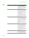
D19 R WRAP 0 Read-only debug field that indicates the last
descriptor in the descriptor list.
D18 R DONE 0 Read-only debug field that indicates the status of
the DONE signal.
D17 R LAST 0 Read-only debug field that indicates the last buffer
descriptor in the current data frame.
D16 R FULL 0 Read-only debug field that indicates the status of
the F bit from the current DMA buffer descriptor.
D15:00 R BLEN 0 Read-only debug field that indicates the current
byte transfer count.
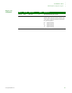
Bit(s) Access Mnemonic Reset Description
13121110987654321015 14
31 29 28 27 26 25 24 23 22 21 20 19 18 17 1630
Not used
Not used SEL


