


. . . . .
PINOUT (265)
General purpose I/O (GPIO)
www.digiembedded.com 31
. . . . . . . . . . . . . . . . . . . . . . . . . . . . . . . . . . . . . . . . . . . . . . . . . . . . . . . . . . . . . . . . . . . . . . . . . . . . . . . . . .
General purpose I/O (GPIO)
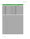
Some signals are multiplexed to two or more GPIOs, to maximize the number of
possible applications. These duplicate signals are marked as (dup) in the
Descriptions column in the table. Selecting the primary GPIO pin and the
duplicate GPIO pin for the same function is not recommended. If both the
primary GPIO pin and duplicate GPIO pin are programmed for the same
function, however, the primary GPIO pin has precedence and will be used.
The I
2
C module must be held in reset until the GPIO assigned to I
2
C has been
configured.
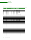
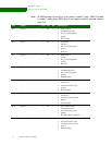
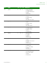
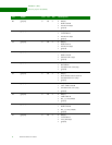
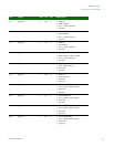
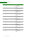
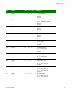
D12 txd[2] / gpio[46] U I/O 2 TX data 2
C12 txd[1] / gpio[45] U I/O 2 TX data 1
B13 txd[0] / gpio[44] U I/O 2 TX data 0
B15 tx_er / gpio[43] U I/O 2 TX code err
B14 tx_en / gpio[42] U I/O 2 TX enable
C14 col / gpio[48] U I/O 2 Collision
C13 crs / gpio[49] U I/O 2 Carrier sense
A14 rx_clk / gpio[34] U I/O 2 RX clock
E17 rxd[3] / gpio[41] U I/O 2 RX data 3
D16 rxd[2] / gpio[40] U I/O 2 RX data 2
B17 rxd[1] / gpio[39] U I/O 2 RX data 1
D13 rxd[0] / gpio[38] U I/O 2 RX data 0
C17 rx_er / gpio[37] U I/O 2 RX error
D17 rx_dv / gpio[36] U I/O 2 RX data valid
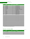
Pin Signal U/D I/O OD Description