. . . . .
WORKING WITH THE CPU
System control processor (CP15) registers
www.digiembedded.com 85
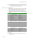
Note:
In all cases, reading from or writing any data values to any CP15 registers,
including those fields specified as
UNPREDICTABLE, SHOULD BE ONE, or SHOULD
BE ZERO,
does not cause any physical damage to the chip.
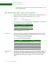
Register summary CP15 uses 16 registers.
Register locations 0, 5, and 13 each provide access to more than one register.
The register accessed depends on the value of the
opcode_2 field in the CP15
MRC/MCR instructions (see “Accessing CP15 registers” on page 83).
Register location 9 provides access to more than one register. The register
accessed depends on the value of the
CRm field (see “Accessing CP15 registers”
on page 83).
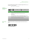
All CP15 register bits that are defined and contain state are set to 0 by reset, with
these exceptions:
The V bit is set to 0 at reset if the VINITHI signal is low, and set to 1 if the
VINITHI signal is high.
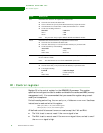
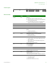
Register Reads Writes
0 ID code (based on
opcode_2 value) Unpredictable
0 Cache type (based on opcode_2 value) Unpredictable
1 Control Control
2 Translation table base Translation table base
3 Domain access control Domain access control
4 Reserved Reserved
5 Data fault status (based on opcode_2 value) Data fault status (based on opcode_2 value)
6 Instruction fault status (based on opcode_2
value)
Instruction fault status (based on opcode_2
value)
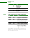
7 Cache operations Cache operations
8 Unpredictable TLB
9 Cache lockdown (based on
CRm value) Cache lockdown
10 TLB lockdown TLB lockdown
11 and 12 Reserved Reserved
13 FCSE PID (based on
opcode_2 value)
FCSE = Fast context switch extension
PID = Process identifier
FCSE PID (based on opcode_2 value)
FCSE = Fast context switch extension
PID = Process identifier
13 Context ID (based on
opcode_2 value) Context ID (based on opcode_2 value)
14 Reserved Reserved
15 Test configuration Test configuration


