


. . . . .
SERIAL CONTROL MODULE: SPI
Interrupt Enable register
www.digiembedded.com 441
Use this register to define the data rate of the interface.
This register must be programmed in three steps. Failure to follow these steps can
result in unpredictable behavior of the SPI module.
Register
programming
steps
1 Set the ENABLE field to 0. The DIVISOR field must not be changed.
2 Set the DIVISOR field to the value you want.
3 Set the ENABLE field to 1. The DIVISOR field must not be changed.
Register
Register bit
assignment
. . . . . . . . . . . . . . . . . . . . . . . . . . . . . . . . . . . . . . . . . . . . . . . . . . . . . . . . . . . . . . . . . . . . . . . . . . . . . . . . . .
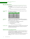
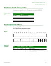
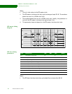
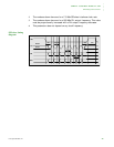
Interrupt Enable register
Address: 9003_1020
13121110987654321015 14
31 29 28 27 26 25 24 23 22 21 20 19 18 17 1630
Not used
Not used
EN
ABL E
Divi sor
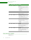
Bit(s) Access Mnemonic Reset Divisor
D31:17 R/W Not used 0 Write this field to 0.
D16 R/W ENABLE 0 Enable clock generation
Write a 1 to this field to enable the SPI module clock
generation logic.
D15:10 R/W Not used 0 Write this field to 0.
D09:00 R/W DIVISOR 0 Divisor
Allows you to specify the required data rate of the
interface. The reference clock used is the system PLL
output. This frequency is a nominal 300 MHz.
For SPI master operation — Set this field to a value
no smaller than 0x009. This produces the maximum
supported data rate of 33 Mbps.
For SPI slave operation — Always set this field to
0x006.