. . . . .
MEMORY CONTROLLER
Address connectivity
www.digiembedded.com 223
Memory banks
constructed from
16-or 32-bit
memory devices
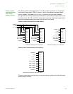
For memory banks constructed from 16- or 32-bit memory devices, it is important
that the byte lane select (PB) bit is set to 1 within the respective memory bank
control register. This asserts all
data_mask[3:0] lines low during a read access as,
during a read, all device bytes must be selected to avoid undriven byte lanes on the
read data value. With 16- and 32-bit wide memory devices, byte select signals exist
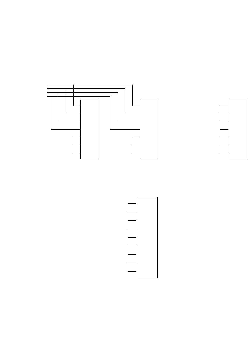
and must be appropriately controlled; see the next two figures.
Memory banks constructed from 16-bit memory
Memory bank constructed from 32-bit memory
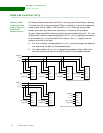
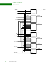
The next figure shows connections for a typical memory system with different data
width memory devices.
32-bit bank consisting of two 16-bit devices 16-bit bank consisting of one 16-bit device
A[20:0]
CE_n
OE_n
WE_n
IO[15:0]
LB_n
UB_n
A[20:0]
CE_n
OE_n
WE_n
IO[15:0]
LB_n
UB_n
A[20:0]
CE_n
OE_n
WE_n
IO[15:0]
LB_n
UB_n
st_oe_n
addr[22:2]
cs[n]
st_we_n
data_mask[2]
data[31:16
data_mask[3]
data_mask[0]
data[15:0]
data_mask[1]
data_mask[2]
data[15:0]
st_oe_n
addr[21:1]
cs[n]
st_we_n
data_mask[3]
32-bit bank consisting of one 32-bit device
data_mask[2]
data[31:0]
st_oe_n
addr[22:2]
cs[n]
st_we_n
data_mask[3]
A[20:0]
CE_n
OE_n
WE_n
IO[31:0]
B[3]_n
B[2]_n
B[1]_n
B[0]_n
data_mask[1]
data_mask[0]


