


EXTERNAL DMA
Control and Status registers
346 Hardware Reference NS9215
. . . . . . . . . . . . . . . . . . . . . . . . . . . . . . . . . . . . . . . . . . . . . . . . . . . . . . . . . . . . . . . . . . . . . . . . . . . . . . . . . .
Control and Status registers
The external DMA configuration registers are located at base address 0xA080_0000.
All the configuration registers are accessed with zero wait states.
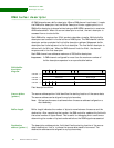
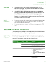
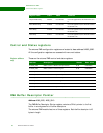
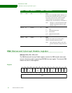
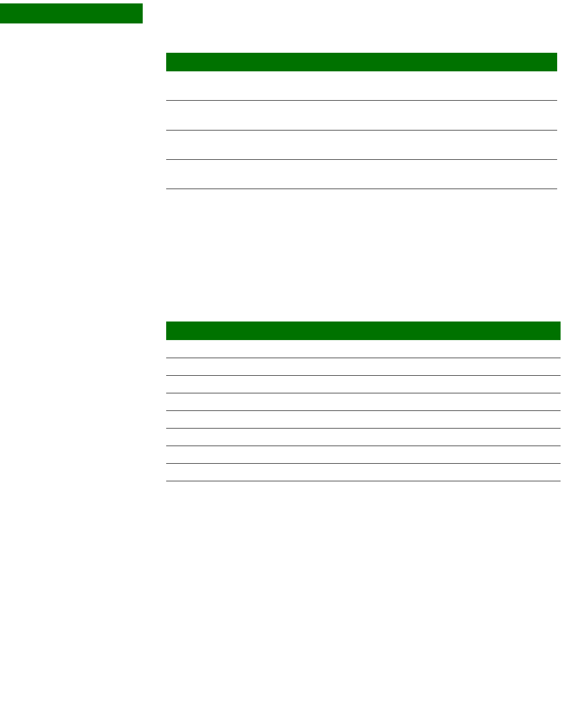
Register address
map
These are the external DMA control and status registers.
. . . . . . . . . . . . . . . . . . . . . . . . . . . . . . . . . . . . . . . . . . . . . . . . . . . . . . . . . . . . . . . . . . . . . . . . . . . . . . . . . .
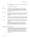
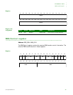
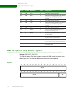
DMA Buffer Descriptor Pointer
Address: A080_0000, A080_0010
The DMA Buffer Descriptor Pointer register contains a 32-bit pointer to the first
buffer in a contiguous list of buffer descriptors.
The external DMA module has two of these registers. Each buffer descriptor is 16
bytes in length.
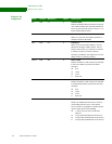
Output Enable Delay WOEN User-defined For most applications, this field can be set to
0.
Write Enable Delay WWEN User-defined For most applications, this field can be left in
the default state.
Write Delay WTWR User-defined For most applications, this field can be left in
the default state.
Turn Delay WTTN User-defined For most applications, this field can be left in
the default state.
Register name Field Value Comment
Address Description Access Reset value
0xA080_0000 DMA Channel 1 Buffer Descriptor Pointer R/W 0x00000000
0xA080_0004 DMA Channel 1 Control register R/W 0x00000000
0xA080_0008 DMA Channel 1 Status and Interrupt Enable R/W 0x00000000
0xA080_000C DMA Channel 1 Peripheral Chip Select R/W 0x00000000
0xA080_0010 DMA Channel 2 Buffer Descriptor Pointer R/W 0x00000000
0xA080_0014 DMA Channel 2 Control register R/W 0x00000000
0xA080_0018 DMA Channel 2 Status and Interrupt Enable R/W 0x00000000
0xA080_001C DMA Channel 2 Peripheral Chip Select R/W 0x00000000