


. . . . .
SERIAL CONTROL MODULE: UART
Receive Buffer GAP Control register
www.digiembedded.com 399
. . . . . . . . . . . . . . . . . . . . . . . . . . . . . . . . . . . . . . . . . . . . . . . . . . . . . . . . . . . . . . . . . . . . . . . . . . . . . . . . . .
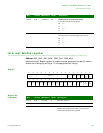
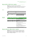
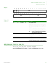
Receive Buffer GAP Control register
Address: 9001_1010 / 9001_9010 / 9002_1010 / 9002_9010
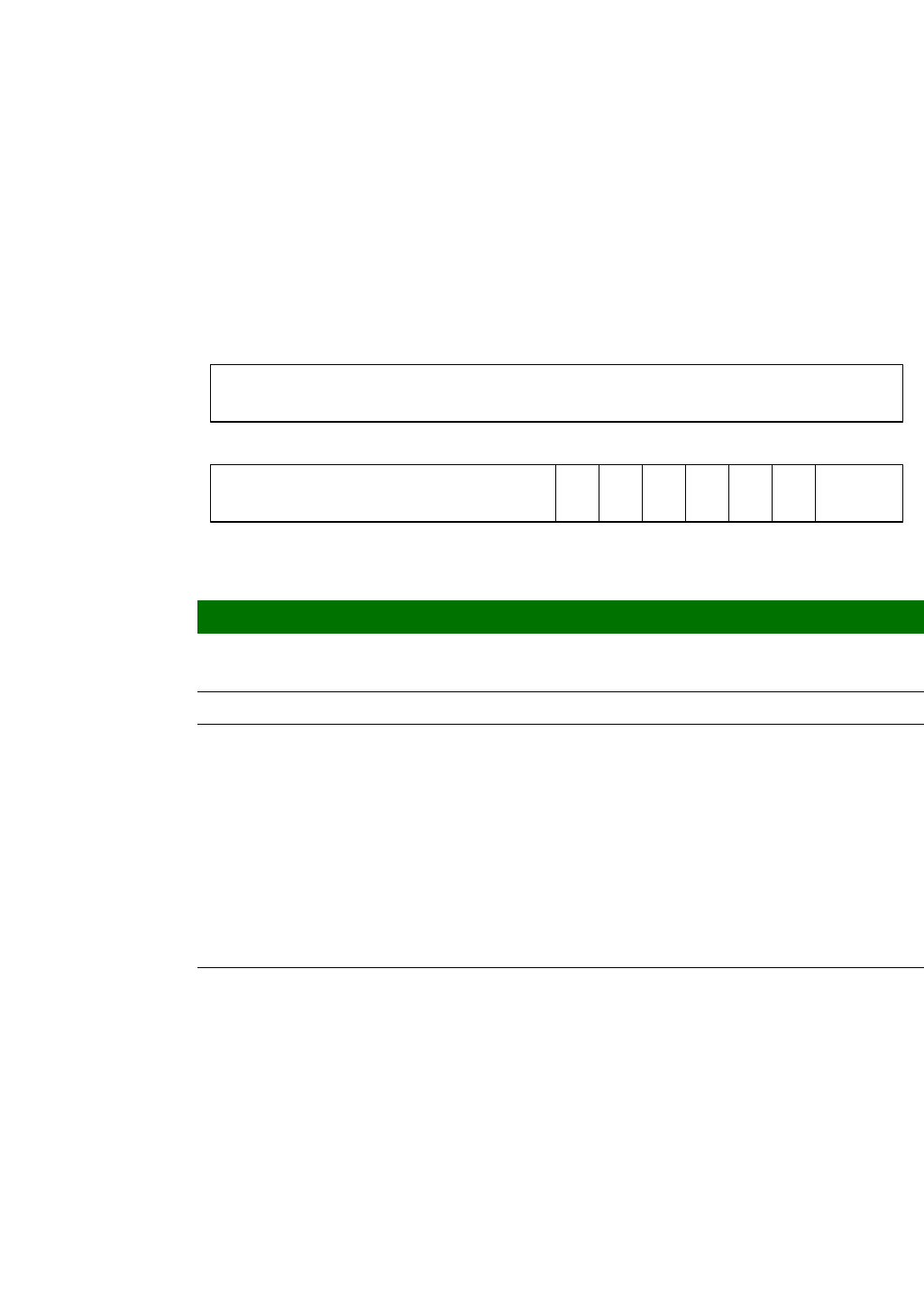
The Receive Buffer GAP Control register configures the receive buffer gap control
logic. The buffer gap timer starts when the first character in a new buffer is
received.
Register
Register bit
assignment
. . . . . . . . . . . . . . . . . . . . . . . . . . . . . . . . . . . . . . . . . . . . . . . . . . . . . . . . . . . . . . . . . . . . . . . . . . . . . . . . . .
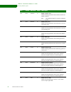
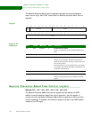
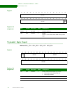
Receive Character Match Control register
Addresses: 9001_1014 / 9001_1018 / 9001_901C / 9001_9020 / 9001_1024 /
9001_9014 / 9001_9018 / 9001_901C / 9001_9020 / 9001_9024 / 9002_1014 /
9002_1018 / 9002_101C / 9002_1020 / 9002_1024 / 9002_9014 / 9002_9018 /
9002_901C / 9002_9020 / 9002_9024
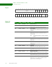
13121110987654321015 14
31 29 28 27 26 25 24 23 22 21 20 19 18 17 1630
Reserved
Reserved
STB WLSPENEPSSPSBDLAB
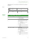
Bits Access Mnemonic Reset Description
D31 R/W ENABLE 0 Enable transmit bit rate generation
Write a 1 to enable the transmit bit rate generator.
D30:25 R/W Not used 0x0 Write this field to 0.
D24:00 R/W VALUE 0 Value
Defines the period between receiving the stop bit and
asserting the buffer gap timeout event.
Use this equation to compute the required divisor value:
N = ((FCLK * gap_period) - 1)
F
CLK
= Nominal 29.4912 Mhz
gap_period = Desired buffer gap period
A reasonable setting is 64 character or 640 bit periods.
GIven a data rate of 115,200 bps, the desired period is
5.55ms and the timeout value is 163,839
d
.