. . . . .
MEMORY CONTROLLER
Byte lane control
www.digiembedded.com 221
. . . . . . . . . . . . . . . . . . . . . . . . . . . . . . . . . . . . . . . . . . . . . . . . . . . . . . . . . . . . . . . . . . . . . . . . . . . . . . . . . .
Byte lane control
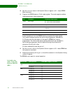
The memory controller generates the byte lane control signals data_mask[3:0]
according to these attributes:
Little or big endian operation
Transfer width
External memory bank databus width, defined within each control register
The decoded address value for write accesses only
Word transfers are the largest size transfers supported by the memory controller.
Any access tried with a size greater that a word causes an error response. Each
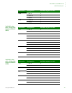
memory chip select can be 8, 16, or 32 bits wide. The memory type used
determines how the st_we_n and data_mask signals are connected to provide byte,
halfword, and word access.
For read accesses, you must control the
data_mask signals by driving them all high or
all low. Do this by programming the byte lane state (PB) bit in the Static
Configuration [3:0] register. See “Address connectivity” on page 222 for additional
information, with respect to
st_we_n and data_mask, for different memory
configurations.
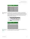
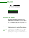
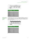
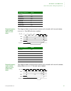
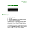
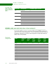
Timing parameters Value
WAITRD 0
WAITOEN 0
WAITPAGE N/A
WAITWR 0
WAITWEN 0
WAITTURN 2


