ANALOG-TO-DIGITAL CONVERTER (ADC) MODULE
ADC DMA procedure
474 Hardware Reference NS9215
ADC control
block
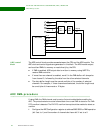
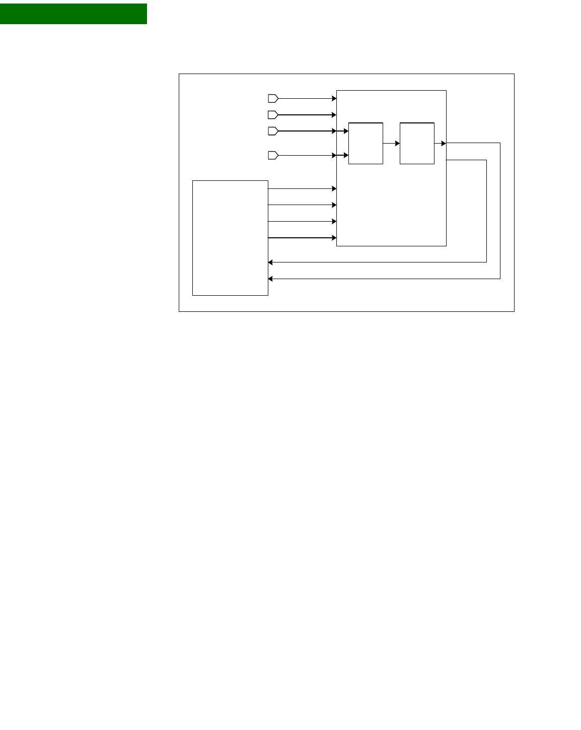
The ADC control block provides access between the CPU and the ADC module. The
ADC clock and control signals are generated in this block. The ADC module output
can be either DMA’d to memory or read directly by the CPU.
If DMA is enabled, ADC output data is written to memory using UART D’s
receive DMA controller.
If more than one channel is enabled, word 0 in the DMA buffer will always be
from channel 0, followed by the data from the other selected channels.
The data buffer length must be a word multiple of the number of selected
channels. For example, if three channels are selected, the buffer length must
be a multiple of three words or 12 bytes.
. . . . . . . . . . . . . . . . . . . . . . . . . . . . . . . . . . . . . . . . . . . . . . . . . . . . . . . . . . . . . . . . . . . . . . . . . . . . . . . . . .
ADC DMA procedure
If using DMA, the DMA channel must be set up first and enabled before enabling the
ADC. The procedure below must be followed each time a new DMA is started or if a DMA
FIFO overflow is detected. The RX FIFO overflow interrupt should be enabled to detect an
overflow.
1 Configure the ADC Configuration register at address 9003 9000 for DMA operation
(bit 3 set to 1) and the number of channels but leave bit 31 set to a 0.
ADC
vref_gnd
vin_0
vref
vin_7
.
.
.
dout[11:0]
ADC Control
adc_clk
sel[2:0]
adc_reset
start
done
SAR
ADC
8:1
MUX


