


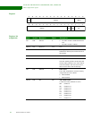
TIMING
Memory Timing
484 Hardware Reference NS9215
. . . . . . . . . . . . . . . . . . . . . . . . . . . . . . . . . . . . . . . . . . . . . . . . . . . . . . . . . . . . . . . . . . . . . . . . . . . . . . . . . .
Memory Timing
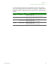
All AC characteristics are measured with 35pF, unless otherwise noted.
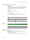
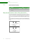
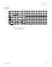
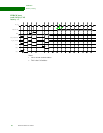
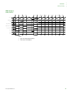
Memory timing contains parameters and diagrams for both SDRAM and SRAM timing.
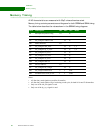
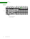
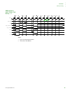
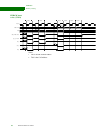
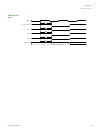
The table below describes the values shown in the SDRAM timing diagrams.
Notes:
1 All four data_mask signals are used for all transfers.
2 All four data_mask signals will go low during a read cycle, for both 16-bit and 32-bit transfers.
3 Only one of the clk_out signals is used.
4 Only one of the dy_cs_n signals is used.
Parm Description Min Max Unit Notes
M1 data input setup time to rising 1.0 ns
M2 data input hold time to rising 0.0 ns
M4 clk_out high to address valid 9.5 ns
M11 address hold time 4.0
M5 clk_out high to data_mask 9.5 ns 1, 2
M6 clk_out high to dy_cs_n low 9.5 ns 3, 4
M7 clk_out high to ras_n low 9.5 ns
M8 clk_out high to cas_n low 9.5 ns
M9 clk_out high to we_n low 9.5 ns
M10 clk_out high to data out 9.5 ns
M12 data out hold time 4.0
M3 clk_out high to clk_en high 9.5 ns
M13 clk_en high to sdram access 2 2 clock
M14 end sdram access to clk_en low 2 2 clocks