. . . . .
WORKING WITH THE CPU
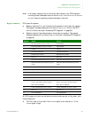
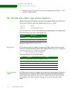
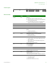
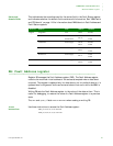
R1: Control register
www.digiembedded.com 89
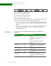
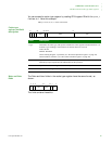
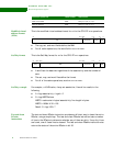
Control register
Bit functionality
131 19 16 15 12 11 10 9 8 7 3 0218 17 14 13 6
S
B
Z
SBZ
S
B
O
S
B
O
L
4
R
R
VI
SBZ
RSB
SBO
CAM
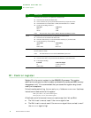
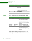
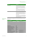
Bits Name Function
[31:19] N/A Reserved:
When read, returns an UNPREDICTABLE value.
When written, SHOULD BE ZERO, or a value read from bits
[31:19] on the same processor.
Use a read-modify-write sequence when modifying this
register to provide the greatest future compatibility.
[18] N/A Reserved, SBO. Read = 1, write =1.
[17] N/A Reserved, SBZ. read = 0, write = 0.
[16] N/A Reserved, SBO. Read = 1, write = 1.
[15] L4 Determines whether the T is set when load instructions change
the PC.
0 Loads to PC set the T bit
1 Loads to PC do not set the T bit
[14] RR bit Replacement strategy for ICache and DCache
0 Random replacement
1 Round-robin replacement
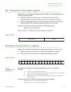
[13] V bit Location of exception vectors
0 Normal exception vectors selected; address range=
0x0000
0000
to 0x0000 001C
1 High exception vectors selected; address range=0xFFFF
0000
to 0xFFFF 001C
Set to the value of VINITHI on reset.
[12] I bit ICache enable/disable
0 ICache disabled
1 ICache enabled
[11:10] N/A
SHOULD BE ZERO
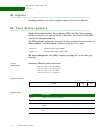
[9] R bit ROM protection
Modifies the ROM protection system.
[8] S bit System protection
Modifies the MMU protection system. See
"MemoryManagement Unit (MMU)," beginning on page 105.
[7] B bit Endianness
0 Little endian operation
1 Big endian operation
Set to the value of
BIGENDINIT on reset.


