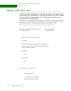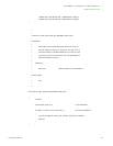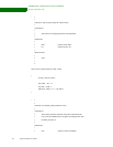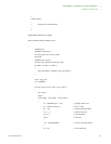
EXTERNAL DMA
Peripheral DMA read access
342 Hardware Reference NS9215
. . . . . . . . . . . . . . . . . . . . . . . . . . . . . . . . . . . . . . . . . . . . . . . . . . . . . . . . . . . . . . . . . . . . . . . . . . . . . . . . . .
Peripheral DMA read access
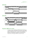
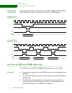
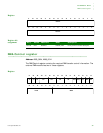
The diagrams in this section describe how the DMA engine performs read accesses of
an external peripheral.
The CLK signal shown is for reference, and its frequency is equal to the speed
grade of the part.
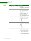
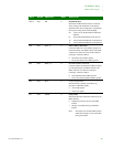
The peripheral data enable signal (PDEN) is an AND function of the active
states of the
st_cs_n[n] and st_oe_n signals.
PDEN timing can be adjusted by the memory controller’s Static Memory
Configuration 0-3 registers, which control
st_cs_n[n] and st_oe_n.
Note:
The PDEN signal is asserted for all accesses on the selected peripheral chip
select. If configuration registers or memory also need to be accessed, you can
use high level address bits and an external gate to disable the PDEN signal.
You can also place the peripheral and configuration registers on separate chip
selects to avoid the need for the external gate.
Determining the
width of PDEN
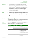
DMA read accesses from an external peripheral are treated as asynchronous
operations by the chip. It is critical that the necessary width of the PDEN assertion
be computed correctly and programmed in the static memory controllers.
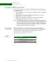
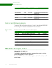
Use this equation to compute total access time:
Total access time = T
a
+ T
b
+T
c
+ 10.0
Equation
variables
Variable Definition
T
a
Peripheral read access time
T
b
Total board propagation delay including buffers
T
c
One AHB CLK cycle period


