


MEMORY CONTROLLER
Address connectivity
222 Hardware Reference NS9215
. . . . . . . . . . . . . . . . . . . . . . . . . . . . . . . . . . . . . . . . . . . . . . . . . . . . . . . . . . . . . . . . . . . . . . . . . . . . . . . . . .
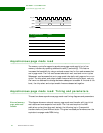
Address connectivity
Memory banks
constructed from
8-bit or non-byte-
partitioned
memory devices
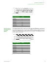
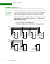
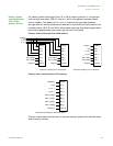
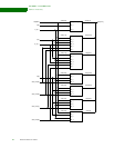
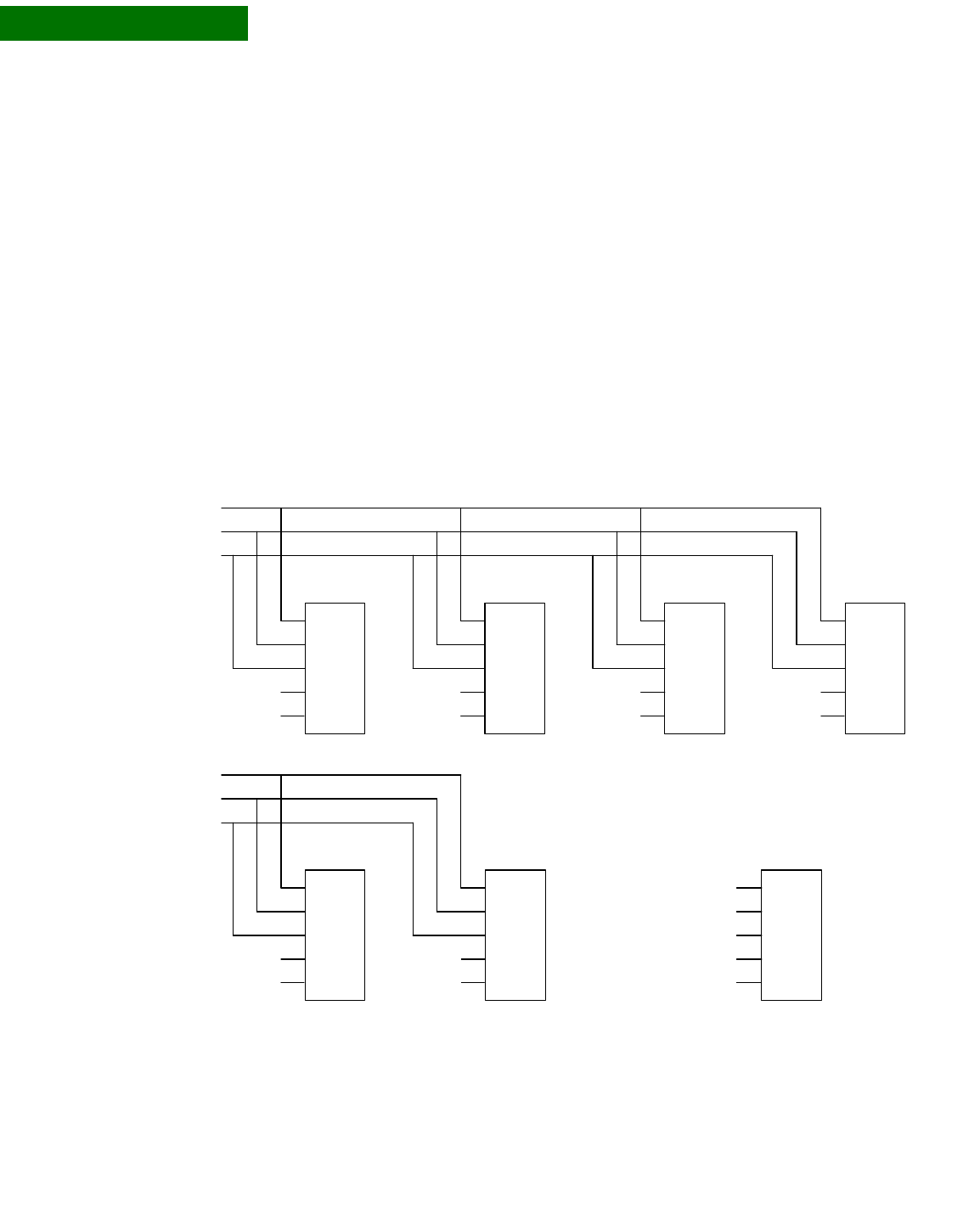
For memory banks constructed from 8-bit or non-byte-partitioned memory devices,
it is important that the byte lane state (PB) bit is cleared to 0 within the respective
memory bank control register. This forces all
data_mask lines high during a read
access, as the byte lane selects are connected to the device write enables.
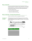
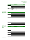
The next figure shows 8-bit memory configuring memory banks that are 8-, 16-, and
32-bits wide. In each of these configurations, the
data_mask[3:0] signals are connected
to write enable (
WE_n) inputs of each 8-bit memory. The st_we_n signal from the
memory controller is not used.
For write transfers, the appropriate data_mask[3:0] byte lane signals are asserted
low, and direct the data to the addressed bytes.
For read transfers, all data_mask[3:0] signals are deasserted high, enabling the
external bus to be defined for at least the width of the accessed memory.
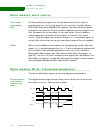
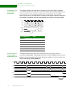
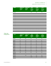
32-bit bank consisting of four 8-bit devices
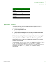
16-bit bank consisting of two 8-bit devices
A[20:0]
CE_n
OE_n
WE_n
IO[7:0]
8-bit bank consisting of one 8-bit device
addr[22:2]
cs[n]
st_oe_n
A[20:0]
CE_n
OE_n
WE_n
IO[7:0]
data_mask[3]
data[31:24]
A[20:0]
CE_n
OE_n
WE_n
IO[7:0]
data_mask[2]
data[23:16]
A[20:0]
CE_n
OE_n
WE_n
IO[7:0]
data_mask[1]
data[15:8]
A[20:0]
CE_n
OE_n
WE_n
IO[7:0]
data_mask[0]
data[7:0]
addr[21:1]
cs[n]
st_oe_n
A[20:0]
CE_n
OE_n
WE_n
IO[7:0]
data_mask[3]
data[31:24]
data_mask[2]
data[23:16]
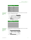
A[20:0]
CE_n
OE_n
WE_n
IO[7:0]
data_mask[3]
data[31:24]
st_oe_n
addr[20:0]
cs[n]