. . . . .
WORKING WITH THE CPU
R9: Cache Lockdown register
www.digiembedded.com 99
Instruction or
data lockdown
register
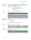
The first four bits of this register determine the L bit for the associated cache way.
The opcode_2 field of the MRC or MCR instruction determines whether the
instruction or data lockdown register is accessed:
Access
instructions
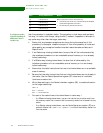
Use these instructions to access the CacheLockdown register.
Modifying the
Cache Lockdown
register
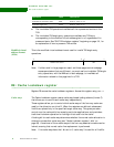
You must modify the Cache Lockdown register using a modify-read-write sequence;
for example:
MRC p15, 0, Rn, c9, c0, 1;
ORR Rn, Rn, 0x01;
MCR p15, 0, Rn, c9, c0, 1;
This sequence sets the L bit to 1 for way 0 of the ICache.
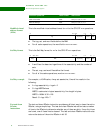
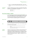
Register format This is the format for the Cache Lockdown register.
Cache Lockdown
register L bits
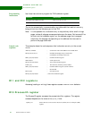
This table shows the format of the Cache Lockdown register L bits. All cache ways
are available for allocation from reset.
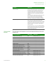
opcode_2=0 Selects the DCache Lockdown register, or the Unified
Cache Lockdown register if a unified cache is
implemented. The ARM926EJ-S processor has separate
DCache and ICache.
opcode_2=1 Selects the ICache Lockdown register.
Function Data Instruction
Read DCache Lockdown register L bits
MRC p15, 0, Rd, c9, c0, 0
Write DCache Lockdown register L bits
MCR p15, 0, Rd, c9, c0, 0
Read ICache Lockdown register L bits
MRC p15, 0, Rd, c9, c0, 1
Write ICache Lockdown register L bits
MCR p15, 0, Rd, c9, c0, 1
31 03
SBZ/UNP
15 416
SB0
L bits
(cache ways
0 to 3)
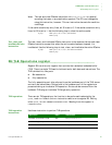
Bits 4-way associative Notes
[31:16] UNP/SBZ Reserved
[15:4] 0xFFF SBO


