


MEMORY CONTROLLER
Dynamic Memory Load Mode register to Active Command Time register
246 Hardware Reference NS9215
Register bit
assignment
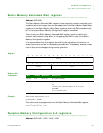
Dynamic Memory Load Mode register to Active Command
. . . . . . . . . . . . . . . . . . . . . . . . . . . . . . . . . . . . . . . . . . . . . . . . . . . . . . . . . . . . . . . . . . . . . . . . . . . . . . . . . .
Time register
Address: A070 0058
The Dynamic Memory Load Mode register to Active Command Time register allows
you to program the Load Mode register to active command time, t
MRD
. It is
recommended that this register be modified during system initialization, or when
there are no current or outstanding transactions. Wait until the memory controller
is idle, then enter low-power or disabled mode. This value normally is found in
SDRAM datasheets as t
MRD
or t
RSA
.
Note:
The Dynamic Memory Load Mode register to Active Command Time register is
used for all four chip selects. The worst case value for all chip selects must be
programmed.
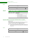
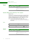
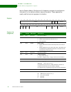
Register
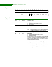
Register bit
assignment
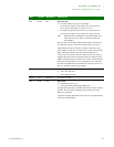
Bits Access Mnemonic Description
D31:04 N/A Reserved N/A (do not modify)
D03:00 R/W RRD Active Bank A to Active Bank B
0x0–0xE
n+1 clock cycles, where the delay is in clk_out cycles
0xF
16 clock cycles (reset on reset_n)
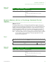
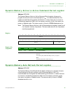
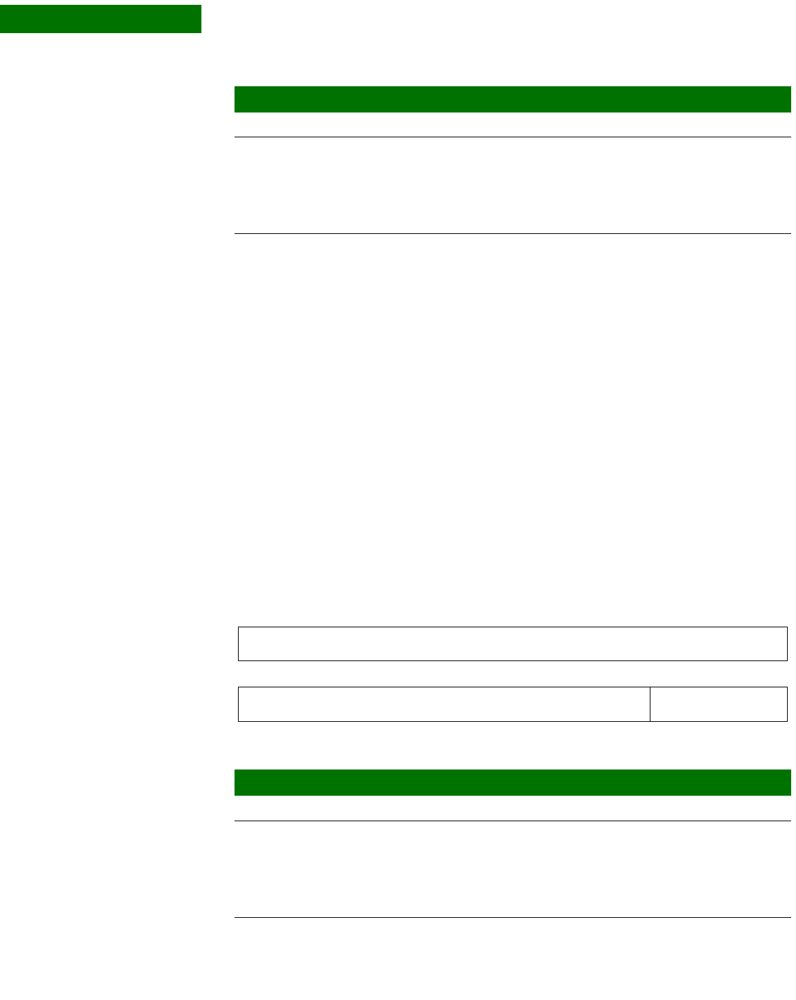
13121110987654321015 14
31 29 28 27 26 25 24 23 22 21 20 19 18 17 1630
Reserved
Reserved MRD
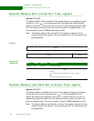
Bits Access Mnemonic Description
D31:045 N/A Reserved N/A (do not modify)
D03:00 R/W MRD Load mode register to Active Command Time
0x0–0xE
n+1 clock cycles, where the delay is in clk_out cycles
0xF
16 clock cycles (reset on reset_n)