MEMORY CONTROLLER
Memory map
206 Hardware Reference NS9215
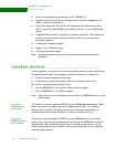
2 When the power-on reset (reset_n) goes inactive, the processor starts booting
from
0x00000000 in memory.
3 The software programs the optimum delay values in the flash memory so the
boot code can run at full speed.
4 The code branches to chip select 1 so the code can continue executing from the
non-remapped memory location.
5 The appropriate values are programmed into the memory controller to
configure chip select 0.
6 The address mirroring is disabled by clearing the address mirror (M) field in the
Control register.
7 The ARM reset and interrupt vectors are copied from flash memory to SRAM that
can then be accessed at address
0x00000000.
8 More boot, initialization, or application code is executed.
Example: Boot
from flash,
SDRAM
remapped after
boot
The system is set up as:
Chip select 1 is connected to the boot flash device.
Chip select 4 is connected to the SDRAM to be remapped to 0x00000000 after
boot.
This is the boot sequence:
1 At power-on, the reset chip select 1 is mirrored into chip select 4 (and chip
select 0).


