MEMORY CONTROLLER
Static memory write control
216 Hardware Reference NS9215
. . . . . . . . . . . . . . . . . . . . . . . . . . . . . . . . . . . . . . . . . . . . . . . . . . . . . . . . . . . . . . . . . . . . . . . . . . . . . . . . . .
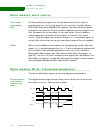
Static memory write control
Write enable
programming
delay
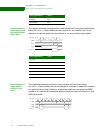
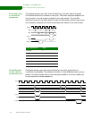
The delay between the assertion of the chip select and the write enable is
programmable from 1 to 16 cycles using the
WA IT WE N bits of the Static Memory
Write Enable Delay (StaticWaitWen[3:0]) registers. The delay reduces the power
consumption for memories. The write enable is asserted on the rising edge of HCLK
after the assertion of the chip select for zero wait states. The write enable is
always deasserted a cycle before the chip select, at the end of the transfer.
datamask_n (byte lane signal) has the same timing as st_we_n (write enable signal) for
writes to 8-bit devices that use the byte lane selects instead of the write enables.
SRAM Write timing for SRAM starts with assertion of the appropriate memory bank chip
selects (
cs[n]_n) and address signals (addr[27:0]_n). The write access time is determined
by the number of wait states programmed for the
WA IT WR field in the Static
Memory Write Delay register (see “Static Memory Write Delay 0–3 registers” on
page 257). The WAITTURN field in the bank control register (see “StaticMemory Turn
Round Delay 0–3 registers” on page 258) determines the number of bus turnaround
wait states added between external read and write transfers.
. . . . . . . . . . . . . . . . . . . . . . . . . . . . . . . . . . . . . . . . . . . . . . . . . . . . . . . . . . . . . . . . . . . . . . . . . . . . . . . . . .
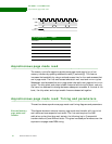
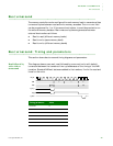
Static memory Write: Timing and parameters
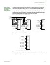
This section shows static memory write timing diagrams and parameters.
External memory
write transfer
with zero wait
states
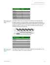
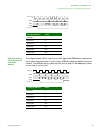
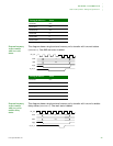
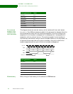
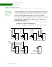
This diagram shows a single external memory write transfer with minimum zero
wait states (
WA IT WR= 0). One wait state is added.
data
cs[n]
clk_out
addr
st_we_n
A
D(A)


