. . . . .
MEMORY CONTROLLER
Bus turnaround
www.digiembedded.com 219
. . . . . . . . . . . . . . . . . . . . . . . . . . . . . . . . . . . . . . . . . . . . . . . . . . . . . . . . . . . . . . . . . . . . . . . . . . . . . . . . . .
Bus turnaround
The memory controller can be configured for each memory bank to use external bus
turnaround cycles between read and write memory accesses. The
WA IT TU RN field
can be programmed for 1 to 16 turnaround wait states, to avoid bus contention on
the external memory databus. Bus turnaround cycles are generated between
external bus transfers as follows:
Read to read (different memory banks)
Read to write (same memory bank)
Read to write (different memory banks)
. . . . . . . . . . . . . . . . . . . . . . . . . . . . . . . . . . . . . . . . . . . . . . . . . . . . . . . . . . . . . . . . . . . . . . . . . . . . . . . . . .
Bus turnaround: Timing and parameters
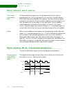
This section shows bus turnaround timing diagrams and parameters.
Read followed by
write with no
turnaround
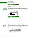
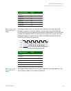
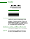
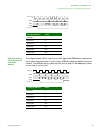
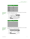
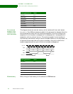
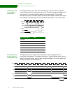
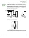
This diagram shows a zero wait read followed by a zero wait write with default
turnaround between the transfers of two cycles because of the timing of the AHB
transfers. Standard AHB wait states are added to the transfers, five for the read and
three for the write.
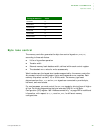
Timing parameter Value
WAITRD 0
WAITOEN 0
WAITPAGE N/A
WAITWR 0
WAITWEN 0
WAITTURN 0
BA 0
D(A) D(B)
clk_out
addr
data
st_oe_n
cs[n]
st_we-n


