


. . . . .
PINOUT (265)
ADC
www.digiembedded.com 49
. . . . . . . . . . . . . . . . . . . . . . . . . . . . . . . . . . . . . . . . . . . . . . . . . . . . . . . . . . . . . . . . . . . . . . . . . . . . . . . . . .
ADC
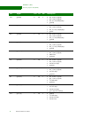
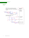
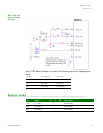
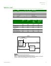
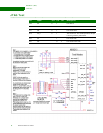
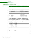
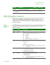
If the ADC feature is not used, the inputs must be terminated as shown below:
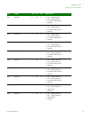
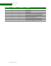
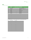
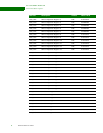
Pin Signal U/D I/O OD Description
P4 agnd_ref_adc Analog reference ground
P5 VREF_adc Analog reference voltage (3.3max
T2 vss_adc ADC_VSS
N6 vdd_adc ADC VDD (3.3V)
R4 vin0_adc I ADC input 0
T3 vin1_adc I ADC input 1
R5 vin2_adc I ADC input 2
U2 vin3_adc I ADC input 3
T4 vin4_adc I ADC input 4
U3 vin5_adc I ADC input 5
T5 vin6_adc I ADC input 6
U4 vin7_adc I ADC input 7
P4 agnd_ref_adc tie to ground
P5 VREF_adc tie to ground
T2 vss_adc tie to ground
N6 vdd_adc tie to 3.3V
R4 vin0_adc tie to ground
T3 vin1_adc tie to ground
R5 vin2_adc tie to ground
U2 vin3_adc tie to ground
T4 vin4_adc tie to ground
U3 vin5_adc tie to ground
T5 vin6_adc tie to ground
U4 vin7_adc tie to ground