MEMORY CONTROLLER
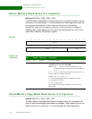
Static Memory Read Delay 0–3 registers
256 Hardware Reference NS9215
. . . . . . . . . . . . . . . . . . . . . . . . . . . . . . . . . . . . . . . . . . . . . . . . . . . . . . . . . . . . . . . . . . . . . . . . . . . . . . . . . .
Static Memory Read Delay 0–3 registers
Address: A070 020C / 022C / 024C / 026C
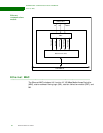
The Static Memory Read Delay 0–3 registers allow you to program the delay from the
chip select to the read access. It is recommended that these registers be modified
during system initialization, or when there are no current or outstanding
transactions. Wait until the memory controller is idle, then enter low-power or
disabled mode. These registers are not used if the extended wait bit is set in the
related Static Memory Configuration register.
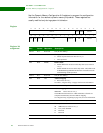
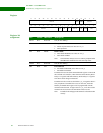
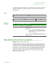
Register
Register bit
assignment
. . . . . . . . . . . . . . . . . . . . . . . . . . . . . . . . . . . . . . . . . . . . . . . . . . . . . . . . . . . . . . . . . . . . . . . . . . . . . . . . . .
StaticMemory Page Mode Read Delay 0–3 registers
Address: A070 0210 / 0230 / 0250 / 0270
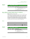
The Static Memory Page Mode Read Delay 0–3 registers allow you to program the
delay for asynchronous page mode sequential accesses. These registers control the
overall period for the read cycle. It is recommended that these registers be
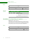
13121110987654321015 14
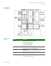
31 29 28 27 26 25 24 23 22 21 20 19 18 17 1630
Reserved
Reserved WTRD
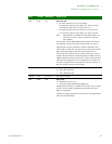
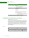
Bits Access Mnemonic Description
D31:05 N/A Reserved N/A (do not modify)
D04:00 R/W WTRD Nonpage mode read wait states or asynchronous page mode
read first access wait state (WAITRD)
00000–11110 (n+1) clk_out cycle for read accesses. For
nonsequential reads, the wait state time is (WAITRD+1) x
t
clk_out
11111 32 clk_out cycles for read accesses (reset value on reset_n)
Use this equation to compute this field:
WTRD = ([T
b
+ T
a
+ 10.0] / T
c
) - 1
T
b
= Total board propagation delay, including any buffers
T
a
= Peripheral access time
T
c
= clk_out clock period.
Any decimal portion must be rounded up. All values are in
nanoseconds


