


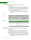

MEMORY CONTROLLER
Dynamic Memory Configuration 0–3 registers
248 Hardware Reference NS9215
Use the Dynamic Memory Configuration 0–3 registers to program the configuration
information for the relevant dynamic memory chip select. These registers are
usually modified only during system initialization.
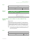
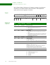
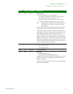
Register
Register bit
assignment
Rsvd
13121110987654321015
14
Rsvd AM
31 29 28 27 26 25 24 23 22 21 20 19 18 17 1630
Reserved Protect BDMC Reserved
AM1 Reserved MD Reserved
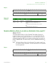
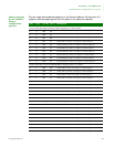
Bits Access Mnemonic Description
D31:21 N/A Reserved N/A (do not modify)
D20 R/W Protect Write protect
0 Writes not protected (reset value on
reset_n)
1 Write protected
D19 R/W BDMC Buffer enable
0 Buffer disabled for accesses to this chip select (reset value on
reset_n)
1 Buffer enabled for accesses to this chip select. The buffers must
be disabled during SDRAM initialization. The buffers must be
enabled during normal operation.
D18:15 N/A Reserved N/A (do not modify)
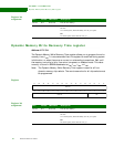
D14 R/W AM Address mapping
0 Reset value on reset_n
See Table , “Register map,” on page 230 for more information.
D13 N/A Reserved N/A (do not modify)
D12:07 R/W AM1 Address mapping
00000000 Reset value on
reset_n
The SDRAM column and row width and number of banks are
computed automatically from the address mapping.
See "Register map," beginning on page 230, for more information.
D06:05 N/A Reserved N/A (do not modify)
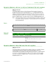
D04:03 R/W MD Memory device
00 SDRAM (reset value on
reset_n)
01 Low-power SDRAM
10 Reserved
11 Reserved
D02:00 N/A Reserved N/A (do not modify)