


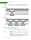


EXTERNAL DMA
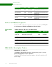
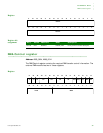
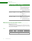
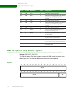
DMA Control register
348 Hardware Reference NS9215
Register bit
assignment
Bit(s) Access Mnemonic Reset Description
D31 R/W CE 0 Channel enable
Enables and disables DMA operations as required.
After a DMA channel has entered the IDLE state
for any reason, this field must be written to a 1 to
initiate further DMA transfers.
D30 R/W CA 0 Channel abort
When set, causes the current DMA operation to
complete and closes the buffer.
D29 R/W CG 0 Channel go
When set, causes the DMA channel to exit the
IDLE state and begin a DMA transfer. The CE
field 31) must also be set, which allows software
to initiate a memory-to-memory transfers.
The dma_req and dma_done signals are not used
during memory-to-memory transfers.
D28:27 R/W SW 0 Source width
Defines the data bus width of the device attached
to the source address specified in the buffer
descriptor.
00 8 bit
01 16 bit
10 32 bit
11 Reserved
D26:25 R/W DW 0 Destination width
Defines the data bus width of the device attached
to the destination address specified in the buffer
descriptor.
00 8 bit
01 16 bit
10 32 bit
11 Reserved
D24:23 R/W SB 0 Source burst
Defines the AHB maximum burst size allowed
when reading from the source. Note that the
source must have enough data, as defined by this
register setting, before asserting REQ.
00 1 unit as set by the source width field
(D28:27)
01 4 bytes (Recommended for 8-bit devices)
10 16 bytes (Recommended for 16-bit devices)
11 32 bytes (Recommended for 32-bit devices)