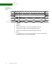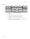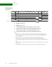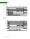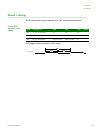
TIMING
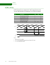
Memory Timing
506 Hardware Reference NS9215
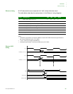
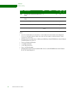
Notes:
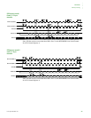
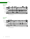
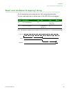
1 Active level of SPI enable is inverted (that is, 1) if the CSPOL bit in Serial Channel Control Register B
is set to a 1. Note that in SPI slave mode, only a value of 0 (low enable) is valid; the SPI slave is fixed
to an active low chip select.
2 SPI data order is reversed (that is, LSB last and MSB first) if the BITORDR bit in Serial Channel
Control Register B is set to a 0.
3 T
BCLK
is period of AHB clock.
4 ± 5% duty cycle skew.
5 ± 10% duty cycle skew.
6 C
load
= 5pf for all outputs.
7 SPI data order can be reversed such that LSB is first. Use the BITORDR bit in Serial Channel
B/A/C/D Control Register A.
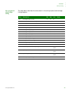
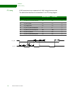
SP22 SPI enable low hold from last SPI CLK in
falling
15 ns 0,3 1
SP23 SPI enable low hold from last SPI CLK in
rising
15 ns 1,2 1
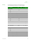
SP24 SPI CLK in high time SP26*40% SP26*60% ns 0,1,2,
3
5
SP25 SPI CLK in low time SP26*40% SP26*60% ns 0,1,2,
3
5
SP26 SPI CLK in period T
BCLK
*8 ns 0,1,2,
3
Parm Description Min Max Unit Mod
es
Not
es


