MEMORY CONTROLLER
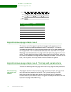
Static memory Write: Timing and parameters
218 Hardware Reference NS9215
Two external
memory write
transfers with
zero wait states
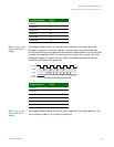
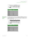
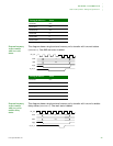
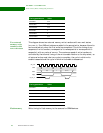
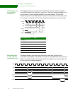
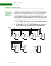
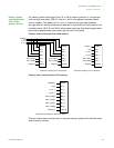
This diagram shows two external memory write transfers with zero wait states
(
WA IT WR= 0). Four AHB wait states are added to the second write, because this write
can be started only when the first write has completed. This is the timing of any
sequence of write transfers, nonsequential to nonsequential or nonsequential to
sequential, with any value of
HBURST. The maximum speed of write transfers is
controlled by the external timing of the write enable relative to the chip select, so
all external writes must take two cycles to complete: the cycle in which write
enable is asserted and the cycle in which write enable is deasserted.
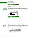
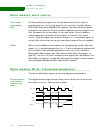
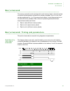
Flash memory Write timing for flash memory is the same as for SRAM devices.
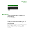
Timing parameters Value
WAITRD N/A
WAITOEN N/A
WAITPAGE N/A
WAITWR 2
WAITWEN 2
WAITTURN N/A
Timing parameter Value
WAITRD N/A
WAITOEN N/A
WAITPAGE N/A
WAITWR 0
WAITWEN 0
WAITTURN 0
A+4A 0
D(A) 0 D(A+4)
clk_out
addr
data
cs[n]
st_we_n


