Hardware Reference Manual 121
Intel
®
IXP2800 Network Processor
Intel XScale
®
Core
3.10.1.1 Read and Write Transactions Initiated by the Intel XScale
®
Core
The Intel XScale
®
core may be used in either a little-endian or big-endian configuration. The
configuration affects the entire system in which the Intel XScale
®
core microarchitecture exists.
Software and hardware must agree on the byte ordering to be used. In software, a system’s
byte order is configured with CP15 register 1, the control register. Bit 7 of this register, the B bit,
informs the processor of the byte order in use by the system. Note that this bit takes effect even if
the MMU is not otherwise in use or enabled. The state of this bit is reflected in the cbiBigEndian
signal.
Although it is the responsibility of system hardware to assign correct byte lanes to each byte field
in the data bus, in the IXP2800 network processor, it is left to the software to interpret byte lanes in
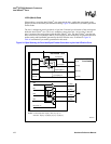
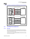
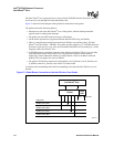
accordance with the endianness of the system. As shown in Figure 24, system byte lanes 0 – 3 are
connected directly to the Intel XScale
®
core byte lanes 0 – 3. This means that byte lane 0 (M[7:0])
of the system is connected to byte lane 0 (X[7:0]) of the Intel XScale
®
core, byte lane 1 (M[15:8])
of the system is connected to byte lane 1 (X[15:8]) of the Intel XScale
®
core, etc.
Interface operation of the Intel XScale
®
core and the rest of the IXP2800 network processor can be
divided into two parts:
• Intel XScale
®
core reading from the IXP2800 network processor
• Intel XScale
®
core writing to the IXP2800 network processor
3.10.1.1.1 Reads Initiated by the Intel XScale
®
Core
Intel XScale
®
core reads can be one of the following three types:
• Byte read
• 16-bits (word) read
• 32-bits (longword) read
Byte Read
When reading a byte, the Intel XScale
®
core generates the byte_enable that corresponds to the
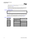
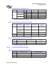
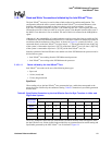
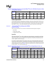
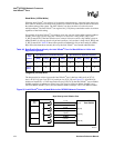
proper byte lane as defined by the endianness setting. Table 45 summarizes byte-enable generation
for this mode.
The 4-to-1 multiplexer steers the byte read into the byte lane 0 location of the read register inside
the Intel XScale
®
core. Select signals for the multiplexer are generated based on endian setting and
ByteEnable generated by the Intel XScale
®
core as defined in Figure 24.
Table 45. Byte-Enable Generation by the Intel XScale
®
Core for Byte Transfers in Little- and
Big-Endian Systems
Byte Number
to be Read
Byte-Enables for Little-Endian System Byte-Enables for Big-Endian System
X_BE[0] X_BE[1] X_BE[2] X_BE[3] X_BE[0] X_BE[1] X_BE[2] X_BE[3]
Byte 0 10000001
Byte 1 01000010
Byte 2 00100100
Byte 3 00011000


