208 Hardware Reference Manual
Intel
®
IXP2800 Network Processor
SRAM Interface
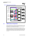
6.2 SRAM Interface Configurations
Memory is logically four bytes (one longword) wide while physically, the data pins are two bytes
wide and double-clocked. Byte parity is supported. Each of the four bytes has a parity bit, which is
written when the byte is written and checked when the longword is read. There are byte-enables
that select the bytes to write, for lengths of less than a longword.
The QDR controller implements a big-endian ordering scheme at the interface pins. For write
operations, bytes 0/1, (data bits [31:16]), and associated parity and byte-enables are written on the
rising edge of the K clock while bytes 2/3, (data bits [15:0]), and associated parity and byte-enables
are written on the rising edge of the K_n clock. For read operations, bytes 0/1, (data bits [31:16]),
and associated parity and byte-enables are captured on the rising edge of CIN0 clock while bytes
2/3, (data bits [15:0]), and associated parity and byte-enables are captured on the rising edge of
CIN0_n clock.
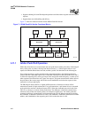
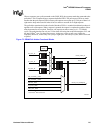
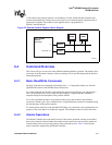
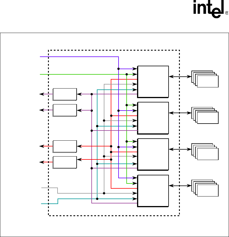
Figure 74. SRAM Controller/Chassis Block Diagram
A8951-01
Push Bus / ID
to ME Cluster 0
Command
Bus from ME
Cluster 0
Command
Bus from ME
Cluster 1
SRAM
Controller
SRAM chips
and/or
co-processor
SRAM
Controller
SRAM
Controller
SRAM
Controller
Push Arb
Push Bus / ID
to ME Cluster 1
Push Arb
Pulll ID to
ME Cluster 0
Pull Arb
Pulll ID to
ME Cluster 1
Pull Data from
ME Cluster 0
Pull Data from
ME Cluster 1
Pull Arb


