194 Hardware Reference Manual
Intel
®
IXP2800 Network Processor
DRAM
5.5.4 Interleaving Across RDRAMs and Banks
In addition to interleaving across the different RDRAM channels, addresses are also interleaved
across RDRAM chips and internal banks. This improves utilization since certain operations to
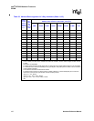
different banks can be performed concurrently. The interleaving is done based on rearranging the
remapped address derived from Section 5.5.1, Section 5.5.2, and Section 5.5.3 as a function of the
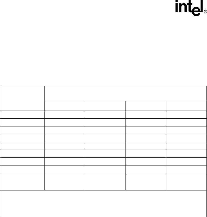
memory size as shown in Table 65. The two MSBs of the rearranged address are used to select
which Bank Command FIFO the command is place in. The rearranged address is also partitioned to
choose RDRAM chip, bank within RDRAM, and page within bank.
5.6 Parity and ECC
DRAM can be optionally protected by byte parity or by an 8-bit error detecting and correcting code
(ECC). RDRAMn_Control[ECC] for each channel selects whether or not that channel should use
Parity, ECC, or no protection. When parity or ECC is enabled x18 RDRAMs must be used with the
extra bits connected to the dqa[8] and dqb[8] signals. Eight bits of ECC code cover eight bytes of
data (aligned to an 8-byte boundary).
5.6.1 Parity and ECC Disabled
• On reads, the data is delivered to the originator of the read; no error is possible.
• Partial writes (writes of less than eight bytes) are done as masked writes.
Table 65. Address Bank Interleaving
Memory Size on
Channel (MB)
3
Remapped Address
Based on RDRAM_Control[Bank_Remap]
00 01 10 11
8 7:14, 22:15 9:14, 7:8, 22:15 11:14, 7:10, 22:15 13:14, 7:12, 22:15
16 7:14, 23:15 9:14, 7:8, 23:15 11:14, 7:10, 23:15 13:14, 7:12, 23:15
32 7:14, 24:15 9:14, 7:8, 24:15 11:14, 7:10, 24:15 13:14, 7:12, 24:15
64 7:14, 25:15 9:14, 7:8, 25:15 11:14, 7:10, 25:15 13:14, 7:12, 25:15
128 7:14, 26:15 9:14, 7:8, 26:15 11:14, 7:10, 2615 13:14, 7:12, 26:15
256 7:14, 27:15 9:14, 7:8, 27:15 11:14, 7:10, 27:15 13:14, 7:12, 27:15
512 7:14, 28:15 9:14, 7:8, 28:15 11:14, 7:10, 28:15 13:14, 7:12, 28:15
1024 7:14, 29:15 9:14, 7:8, 29:15 11:14, 7:10, 29:15 13:14, 7:12, 29:15
Bits used to select
Bank Command
FIFO
7:8 9:10 11:12 13:14
NOTES:
1. Table shows device/bank sorting of the channel remapped block address, which is in address 31:7. LSBs of
the address are always 6:0 (byte within the block), which are not remapped.
2. Unused MSBs of address have value of 0.
3. Size is programmed in RDRAM_Control[Size].


