372 Hardware Reference Manual
Intel
®
IXP2800 Network Processor
Clocks and Reset
10.4.1 Flash ROM
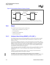
At power up, if FLASH_ROM is present, strap pin CFG_PROM_BOOT should be sampled 1
(should be pulled up). Therefore after reset being removed by the PLL logic from the
IXP_RESET0 register, the Intel XScale
®
core reset is automatically removed. Flash Alias Disable
(bit [8] of Misc Control register) information is used by the Intel XScale
®
core gasket to decide
where to forward address 0 from the Intel XScale
®
core when the Intel XScale
®
core wakes up and
starts accessing the code from address 0. In this mode, since “flash alias disable” bit is reset to 0,
the Intel XScale
®
core gasket will convert access to address 0 to PROM access from address 0
using the CAP command. Based on the code residing inside PROM, the Intel XScale
®
core starts
removing reset from SRAM, PCI, DRAM, Microengines etc. by writing 0 in their corresponding
bit location of IXP_RESETn register and then initializing their configuration registers.
Boot code in PROM can change flash alias disable bit to 1 anytime to map DRAM at address 0 and
therefore block further accesses to PROM at address 0. This change should be done before putting
any data in DRAM at address 0.
The Intel XScale
®
core also sets different BARs inside PCI unit to define memory requirements for
different windows.
The Intel XScale
®
core behavior as a host is controlled by CFG_PCI_BOOT_HOST strap option.
If CFG_PCI_BOOT_HOST is sampled asserted in the de-asserting edge of reset, the Intel XScale
®
core will behave as boot host and configure the PCI system.
10.4.2 PCI Host Download
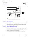
At power up, if FLASH_ROM is not present, strap pin CFG_PROM_BOOT should be sampled 0
(should be pulled down). In this mode CFG_RST_DIR pin should be 0 at power up signaling
PCI_RST_L pin is an input that behaves as global chip reset.
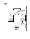
1. Even after reset is removed by the PLL logic from IXP_RESET0 register (after PCI_RST_L
reset is de-asserted), the Intel XScale
®
core reset is not removed.
2. PCI Reset through IXP_RESET0 [16] is removed automatically after being set and reset being
removed.
3. IXP_RESET0[21] is set after PCI_RST_L has been removed and PLL_LOCK is sampled
asserted.
4. Once IXP_RESET0[21] is set, PCI unit starts responding to transactions.
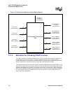
5. PCI Host first configures CSR, SRAM and DRAM base address registers after reading size
requirements for these BARs. The size for CSR, SRAM and DRAM is defined by the use of
Strap pins. Pre-fetchability for the window is defined by bit [3] of the respective BAR
registers; therefore when host reads these registers, bit [3] is returned as 0 for CSR, SRAM and
DRAM defining CSRs and also if SRAM and DRAM are to be non-prefetchable. Type Bits
[2:0] are always Read-Only and return the value of 0x0 when read for CSR, SRAM and
DRAM BAR registers.
6. PCI Host also programs Clock Control CSR, for PLL unit to generate proper clocks for
SRAM, DRAM and other units.
Once these base address registers have been programmed, PCI host programs DRAM channels by
initializing SDRAM_CSR, SDRAM_MEMCTL0, SDRAM_MEMCTL1 and SDRAM_MEMINIT
registers. Once these registers have been programmed, PCI host writes the BOOT Code in DRAM
starting at DRAM address 0. PCI Host can also program other registers if required. Once the boot


