


158 Hardware Reference Manual
Intel
®
IXP2800 Network Processor
Intel XScale
®
Core
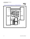
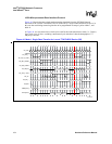
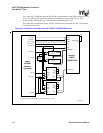
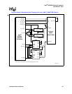
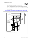
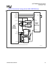
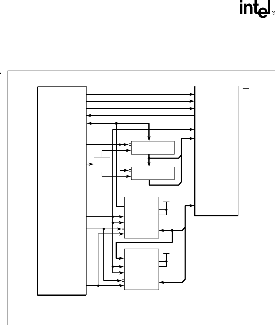
For a write, SP_CP loads the data onto the 74F646 (or equivalent) tri-state buffers, using two clock
cycles. To reduce the pin count, the 16-bit data is latched with the same pin (SP_CS_L[1]),
assuming that a turnaround cycle is inserted between the transaction cycles.
For a read, data are shifted out of two 74F646 or equivalent tri-state buffers by SP_CP, using two
consecutive clock cycles.
Figure 48. An Interface Topology with Intel / AMCC* SONET/SDH Device
A9714-02
SP_RD_L
SP_CS_L[1]
SP_ACK_L
SP_AD[7:0]
CE#
CP
D[7:0]
Q[7:0]
74F377
SP_WR_L
RDB
CSB
INT
WRB
ADDR[9:0]
DATA[15:0]
Intel
®
IXP2800
Network
Processor
Intel
®
or
AMCC*
SONET/SDH
SP_ALE_L
SP_CLK
SP_CP
SP_OE_L
SP_DIR
ALE
CE#
CP
D[7:0]
ADDR[10:8]
ADDR[7:1]
DATA[7:0]
DATA[15:8]
VCC
Q[7:0]
74F377
D[7:0]
CPAB
74F646
DIR
OE#
CPBA
SAB
O[7:0]
SBA
D[7:0]
CPAB
74F646
DIR
OE#
CPBA
SAB
O[7:0]
SBA
VCC
* Other names and brands may be claimed as property of others.
MCUTYPE
VCC
Clock
Driver
CY2305